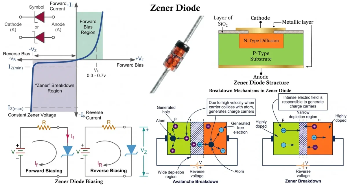
A Zener diode is a specially designed silicon semiconductor diode that is intended to operate in the reverse breakdown region. Unlike an ordinary PN junction diode, which is normally damaged when subjected to excessive reverse voltage, a Zener diode is manufactured with carefully controlled doping concentrations that allow it to safely operate in the breakdown region without damage.
The breakdown voltage of a Zener diode can be precisely controlled during manufacturing and is available in a wide range, typically from 2.4 V to over 200 V. The device is named after physicist Carl Zener, who first explained the breakdown phenomenon occurring in heavily doped PN junctions.
In normal operation, a Zener diode is connected in reverse bias. When the applied reverse voltage reaches the specified Zener breakdown voltage (VZ), the diode begins conducting heavily while maintaining an almost constant voltage across its terminals. This unique characteristic makes Zener diodes ideal for voltage regulation, voltage reference circuits, overvoltage protection, clipping circuits, and power supply stabilization.
Modern electronic systems require stable voltage levels for proper operation. Variations in supply voltage can cause malfunction, reduced performance, or permanent damage to sensitive electronic components. To overcome these issues, Zener diodes are widely used as voltage regulators, providing a simple, reliable, and cost-effective method of maintaining a constant output voltage.

The most important characteristic of a Zener diode is its ability to maintain a nearly constant voltage over a wide range of current variations. This property makes it one of the most widely used semiconductor devices in analog and power electronic circuits.
Related Articles:
- Types of Diodes: Symbol, Working, Characteristics and Applications
- Difference Between Photodiode, Phototransistor and Photoresistor
- Constant Current Diode Symbol, Construction, Working & Applications
- Diode Clipper Circuit Diagram, Types, Working and Applications
- Diode Clamper Circuit Diagram, Types, Working and Applications
- TVS Diode: Symbol, Construction, Working, Types and Applications
- Power Diode: Symbol, Construction, Working, Types & Applications
- Tunnel Diode Symbol, Construction, Working and Applications
- LED – Symbol, Construction, Working, Types and Applications
- Laser Diode – Symbol, Construction, Working, Types & Applications
Symbol of Zener Diode
The symbol of a Zener diode is similar to that of a conventional PN junction diode, except that the cathode line is bent at both ends. This modified cathode symbol indicates that the device is specifically designed to operate in the reverse breakdown region.

A Zener diode consists of two terminals:
- Anode (A): Connected to the P-type semiconductor region.
- Cathode (K): Connected to the N-type semiconductor region and usually identified by a colored band on the device package.
Depending on the applied voltage polarity, a Zener diode can operate in two modes:
- Forward Bias Operation: The Zener diode behaves like an ordinary silicon diode and starts conducting when the forward voltage reaches approximately 0.7 V.
- Reverse Bias Operation: The diode remains non-conducting except for a small leakage current until the reverse voltage reaches the Zener breakdown voltage. Beyond this point, the diode conducts heavily while maintaining an almost constant voltage across its terminals.
Although a Zener diode can operate in both forward and reverse bias conditions, its primary application is in the reverse breakdown region where it acts as a voltage-regulating device.
Construction of Zener Diode
The construction of a Zener diode is similar to that of a conventional PN junction diode, but it is specifically designed to operate in the reverse breakdown region. The most important difference lies in the heavy doping concentration of both the P-type and N-type semiconductor regions, which produces a very thin depletion layer and a precisely controlled breakdown voltage.
Unlike ordinary PN junction diodes that are intended to block reverse current, Zener diodes are optimized to withstand reverse breakdown safely and repeatedly without suffering permanent damage.

Internal Structure
The basic structure of a Zener diode consists of a heavily doped silicon PN junction fabricated using advanced semiconductor manufacturing techniques. The doping concentration is carefully controlled during production to achieve the desired breakdown voltage.
- P-type Semiconductor Region
- The P-type region is heavily doped with trivalent impurities such as boron.
- It contains holes as the majority charge carriers.
- Heavy doping increases the concentration of charge carriers and reduces the width of the depletion region.
- N-type Semiconductor Region
- The N-type region is heavily doped with pentavalent impurities such as phosphorus or arsenic.
- It contains electrons as the majority charge carriers.
- The high doping concentration contributes to the formation of a strong electric field across the junction.
Formation of Depletion Region
When the P-type and N-type semiconductor materials are joined together, electrons from the N-region diffuse into the P-region while holes from the P-region diffuse into the N-region. As a result, recombination occurs near the junction, creating a region depleted of free charge carriers known as the depletion region.
In a Zener diode, both semiconductor regions are heavily doped, causing the depletion layer to become extremely thin compared to that of a conventional diode.
- The depletion layer thickness is very small.
- A strong electric field is established across the junction.
- The junction can reach breakdown at comparatively low reverse voltages.
Why Heavy Doping is Required?
The unique operation of a Zener diode depends on the heavy doping of the PN junction.
- Creates a narrow depletion region.
- Produces a very strong electric field across the junction.
- Allows reverse breakdown to occur at a predetermined voltage.
- Ensures stable voltage regulation characteristics.
- Provides a sharp and well-defined breakdown region.
The breakdown voltage of the diode is controlled by adjusting the doping concentration during manufacturing. Higher doping levels generally result in lower breakdown voltages, while lower doping levels produce higher breakdown voltages.
Electric Field Distribution
Due to the extremely thin depletion layer, a very high electric field is developed across the junction even at relatively low reverse voltages.
The electric field intensity can be expressed as:
E = V / W
- E = Electric field intensity (V/cm)
- V = Applied reverse voltage
- W = Width of depletion region
Since the depletion width W is very small, the electric field becomes extremely high, resulting in Zener or avalanche breakdown.
Ohmic Contacts
Metal contacts are formed on both sides of the semiconductor junction to provide electrical connections.
- Anode Contact: Connected to the P-type region.
- Cathode Contact: Connected to the N-type region.
These contacts are designed to provide low resistance and reliable current flow while minimizing power losses.
Passivation Layer
The semiconductor junction is protected using a passivation layer made of materials such as silicon dioxide (SiO2) or silicon nitride (Si3N4).
This protective layer:
- Prevents contamination and moisture penetration.
- Reduces surface leakage current.
- Improves long-term reliability.
- Maintains stable breakdown characteristics.
Encapsulation and Packaging
After fabrication, the semiconductor chip is enclosed in a protective package to provide mechanical strength and environmental protection.
Common package types include:
- DO-35 Glass Package
- DO-41 Axial Lead Package
- SOD-123 Surface Mount Package
- SOT-23 Surface Mount Package
- Power Zener Packages for high-power applications
The package also assists in heat dissipation and protects the junction from mechanical damage.
Construction Features of Zener Diode
The special construction of a Zener diode enables its unique voltage regulation capability, whereas a PN junction diode is moderately doped, used mainly for rectification, and is usually damaged by reverse breakdown.
- Heavily Doped PN Junction: Produces a thin depletion region and controlled breakdown voltage.
- Narrow Depletion Layer: Allows breakdown to occur at a predetermined reverse voltage.
- Strong Electric Field: Enables Zener or avalanche breakdown mechanisms.
- Precise Doping Control: Ensures accurate and stable breakdown voltage ratings.
- Protective Passivation Layer: Improves reliability and prevents environmental damage.
- Robust Packaging: Provides mechanical protection and efficient heat dissipation.
Working of Zener Diode
A Zener diode is specifically designed to operate in the reverse breakdown region. Unlike an ordinary PN junction diode, which is normally damaged when subjected to excessive reverse voltage, a Zener diode is manufactured with a heavily doped junction that allows it to operate safely in breakdown while maintaining a nearly constant voltage across its terminals.
The working of a Zener diode can be understood by examining its behavior under both forward bias and reverse bias conditions. Although it can conduct in forward bias like a conventional diode, its primary application is in the reverse-biased mode where it functions as a voltage regulator.

Operating Regions of a Zener Diode
- Forward Bias Region: The Zener diode behaves like a normal silicon diode and conducts current when the forward voltage exceeds approximately 0.7 V.
- Reverse Bias Region (Before Breakdown): Only a very small reverse leakage current flows through the diode.
- Reverse Breakdown Region: When the reverse voltage reaches the Zener voltage (VZ), the diode conducts heavily while maintaining an almost constant voltage across its terminals.
Modes of Operation
Forward Bias Operation
When the anode of the Zener diode is connected to the positive terminal of the supply and the cathode is connected to the negative terminal:
- The diode becomes forward biased.
- The depletion region narrows.
- Majority charge carriers cross the junction.
- Current starts flowing through the diode.
- The forward voltage drop is approximately 0.7 V for silicon Zener diodes.
In this condition, the Zener diode behaves exactly like an ordinary silicon PN junction diode and is rarely used for voltage regulation.
Reverse Bias Operation (Before Breakdown)
When the cathode is connected to the positive terminal of the supply and the anode is connected to the negative terminal:
- The diode becomes reverse biased.
- The depletion region widens.
- Majority charge carriers move away from the junction.
- Only a very small reverse saturation current flows.
- The diode behaves almost like an open circuit.
This small reverse current is caused by thermally generated minority charge carriers and is typically in the microampere range.

Reverse Breakdown Operation (Zener Region)
As the reverse voltage is increased further, a point is reached where the electric field across the depletion region becomes extremely strong.
At a specific reverse voltage called the Zener Breakdown Voltage (VZ):
- The depletion region undergoes breakdown.
- The reverse current increases rapidly.
- The voltage across the diode remains almost constant.
- The diode safely conducts large reverse current.
- The diode enters its normal operating region.
This unique property makes the Zener diode an excellent voltage-regulating device.
Zener Knee Point
The point at which the reverse current suddenly increases is called the Zener Knee.
- The voltage corresponding to this point is called the Zener Voltage (VZ).
- The current corresponding to this point is called the Zener Knee Current (IZK) or Minimum Zener Current (IZ(min)).
- The diode must conduct at least this current to maintain proper voltage regulation.
Once the current exceeds the knee current, the voltage across the diode remains nearly constant despite large changes in current.
Voltage Regulation Mechanism
The most important application of a Zener diode is voltage regulation.
When connected in reverse bias with a series current-limiting resistor:
- If the supply voltage increases, the Zener current increases.
- The voltage across the diode remains approximately constant.
- If the load current changes, the Zener current automatically adjusts.
- The output voltage remains stable despite input or load variations.
This automatic adjustment of current enables the Zener diode to maintain a constant output voltage.
Current Limiting Resistor
A series resistor is always connected with a Zener diode to limit the reverse current and prevent damage.
The value of the series resistor can be calculated using:
R = (VIN – VZ) / IZ
- R = Series resistor (Ω)
- VIN = Input supply voltage (V)
- VZ = Zener voltage (V)
- IZ = Zener current (A)
The resistor ensures that the Zener current always remains between:
IZ(min) < IZ < IZ(max)
Operating outside this range may result in poor regulation or damage to the diode.
Current Flow in the Zener Region
In the reverse breakdown region:
- The reverse voltage remains almost constant.
- The current through the diode may vary significantly.
- The internal dynamic resistance of the diode is very small.
- Power is dissipated in the form of heat.
The power dissipated by the Zener diode is given by:
PZ = VZ × IZ
- PZ = Power dissipation (W)
- VZ = Zener voltage (V)
- IZ = Zener current (A)
To ensure safe operation:
PZ ≤ PZ(max)
PZ(max) is the maximum power rating specified by the manufacturer.
- The Zener diode is primarily operated in reverse bias.
- It conducts heavily when the reverse voltage reaches the Zener voltage.
- The voltage across the diode remains nearly constant in the breakdown region.
- A series resistor is required to limit the Zener current.
- It can be used as a voltage regulator, voltage reference, and protection device.
- The diode automatically compensates for changes in supply voltage and load current.
V-I Characteristics of Zener Diode
The V-I (Voltage-Current) characteristics of a Zener diode describe the relationship between the voltage across the diode and the current flowing through it under both forward-bias and reverse-bias conditions. The most important feature of a Zener diode is its ability to operate safely in the reverse breakdown region, where it maintains an almost constant voltage despite large variations in current.
Unlike a conventional PN junction diode, which is normally damaged when operated beyond its reverse breakdown voltage, a Zener diode is specifically designed to utilize the breakdown region for voltage regulation and voltage reference applications.

The V-I characteristics of a Zener diode can be divided into Forward Bias Characteristics and Reverse Bias Characteristics.
Forward Bias Characteristics
When the Zener diode is connected in forward bias, it behaves like a conventional silicon PN junction diode.
- The anode is connected to the positive terminal of the supply.
- The cathode is connected to the negative terminal.
- The depletion region becomes narrow.
- The diode begins conducting after the forward threshold voltage is reached.
- For a silicon Zener diode, the forward voltage drop is approximately 0.7 V.
As the forward voltage increases beyond the threshold value, the forward current increases rapidly while the voltage remains nearly constant.
Reverse Bias Characteristics
The reverse-bias region is the most important operating region of a Zener diode.
When the cathode is connected to the positive terminal and the anode is connected to the negative terminal:
- The diode becomes reverse biased.
- The depletion region widens.
- Only a very small reverse leakage current flows.
- The diode behaves almost like an open circuit.
As the reverse voltage increases further, the diode eventually reaches its breakdown region.
Reverse Leakage Region
Initially, when a small reverse voltage is applied:
- A very small reverse current flows.
- This current is called the reverse leakage or reverse saturation current (I0).
- The leakage current is typically in the microampere (μA) range.
- The diode offers very high resistance in this region.
Since the current is extremely small, the diode effectively behaves as an open circuit.
Zener Breakdown Region
As the reverse voltage approaches the specified breakdown voltage:
- The electric field across the depletion region increases rapidly.
- A point is reached where breakdown occurs.
- The reverse current increases sharply.
- The voltage across the diode remains nearly constant.
This region is called the Zener Breakdown Region and represents the normal operating region of the Zener diode.
Zener Breakdown Voltage (VZ)
The reverse voltage at which breakdown occurs is called the Zener Breakdown Voltage.
- It is represented by VZ.
- It is determined by the doping concentration during manufacturing.
- Typical values range from approximately 2.4 V to over 200 V.
- The voltage remains nearly constant once breakdown begins.
Zener Knee Point
The transition from the leakage region to the breakdown region is called the Zener Knee.
- The knee point indicates the beginning of voltage regulation.
- The voltage corresponding to this point is the Zener voltage.
- The current corresponding to this point is called the knee current.
The sharper the knee, the better the voltage regulation characteristics of the diode.
Zener Knee Current (IZK)
The minimum current required to keep the diode operating in the breakdown region is known as the Zener Knee Current.
- Also called Minimum Zener Current (IZ(min)).
- Represented as IZK.
- The diode must conduct at least this current to maintain voltage regulation.
If the current falls below IZK, the diode may leave the breakdown region and voltage regulation will be lost.
Zener Test Current (IZT)
The current at which the nominal Zener voltage is specified is called the Zener Test Current.
- Represented as IZT.
- Specified in the manufacturer’s datasheet.
- The rated Zener voltage VZ is measured at this current.
Most electrical parameters of the diode are specified at IZT.
Maximum Zener Current (IZM)
The maximum reverse current that the Zener diode can safely carry without damage is called the Maximum Zener Current.
- Represented as IZM or IZ(max).
- Determined by the power dissipation capability of the diode.
- Exceeding this current may cause overheating and permanent damage.
The operating condition must satisfy:
IZK ≤ IZ ≤ IZM
Dynamic Resistance of Zener Diode
Ideally, the Zener breakdown characteristic should be perfectly vertical. However, in practice, a small increase in voltage occurs when the Zener current increases.
This behavior is represented by the dynamic resistance or Zener impedance.
The dynamic resistance is defined as:
ZZ = ΔVZ / ΔIZ
- ZZ = Dynamic Zener Resistance (Ω)
- ΔVZ = Change in Zener Voltage (V)
- ΔIZ = Change in Zener Current (A)
A lower dynamic resistance indicates better voltage regulation performance.
Power Dissipation in Zener Region
When operating in the breakdown region, the diode dissipates power in the form of heat.
The power dissipation is given by:
PZ = VZ × IZ
- PZ = Zener Power Dissipation (W)
- VZ = Zener Voltage (V)
- IZ = Zener Current (A)
For safe operation:
PZ ≤ PZ(max)
where PZ(max) is the maximum power rating specified by the manufacturer.
Important V-I Characteristic Parameters
- VZ (Zener Voltage): Reverse breakdown voltage of the diode.
- IZK (Knee Current): Minimum current required for proper regulation.
- IZT (Test Current): Current at which VZ is specified.
- IZM (Maximum Current): Maximum safe operating current.
- ZZ (Dynamic Resistance): Small-signal resistance in the breakdown region.
- PZ(max): Maximum permissible power dissipation.
The sharp reverse breakdown characteristic and nearly constant voltage in the breakdown region make the Zener diode one of the most widely used devices for voltage regulation, voltage reference generation, and overvoltage protection circuits.
Breakdown Mechanisms in Zener Diode
The most important characteristic of a Zener diode is its ability to operate safely in the reverse breakdown region. When the reverse voltage across the diode exceeds a certain critical value, the reverse current increases rapidly while the voltage across the diode remains nearly constant.
This breakdown occurs due to two distinct physical mechanisms Zener Breakdown and Avalanche Breakdown. The type of breakdown that occurs depends mainly on the doping concentration and the width of the depletion region.

For commercially available Zener diodes:
- Zener breakdown generally occurs for breakdown voltages below approximately 5 V to 6 V.
- Avalanche breakdown generally occurs for breakdown voltages above approximately 6 V.
- Between approximately 5 V and 8 V, both mechanisms may contribute simultaneously.
Although the physical mechanisms are different, all such devices are commonly referred to as Zener diodes.
Zener Breakdown
Zener breakdown occurs in heavily doped PN junctions having a very thin depletion region. When a reverse voltage is applied across the diode, an extremely strong electric field is developed across the narrow depletion layer.
As the reverse voltage increases, the electric field intensity becomes sufficiently large to pull valence electrons away from their parent atoms. This process breaks the covalent bonds and generates a large number of free electrons and holes.
As a result, the reverse current increases suddenly and the diode enters the breakdown region.
Working of Zener Breakdown
- The PN junction is heavily doped.
- The depletion region becomes extremely thin.
- A strong electric field develops across the junction.
- Valence electrons are pulled out of their covalent bonds.
- Large numbers of electron-hole pairs are generated.
- The reverse current increases abruptly.
- The diode enters the breakdown region and maintains an almost constant voltage.
Characteristics of Zener Breakdown
- Occurs in heavily doped PN junctions.
- Associated with a very thin depletion region.
- Typically occurs below 5 V to 6 V.
- Produces a sharp breakdown characteristic.
- Has a negative temperature coefficient.
- Breakdown voltage decreases as temperature increases.
Effect of Temperature on Zener Breakdown
As the junction temperature increases, the covalent bonds become weaker and require less energy to break.
Temperature ↑ → Breakdown Voltage ↓
This negative temperature coefficient is one of the distinguishing features of Zener breakdown.
Avalanche Breakdown
Avalanche breakdown occurs in lightly doped PN junctions having a wider depletion region. In this case, breakdown is caused by a process known as impact ionization or carrier multiplication.
When a sufficiently high reverse voltage is applied, the minority charge carriers gain large kinetic energy while moving through the depletion region. These high-speed carriers collide with atoms in the crystal lattice and knock out valence electrons.
Each collision generates a new electron-hole pair. These newly generated carriers are also accelerated by the electric field and create additional electron-hole pairs through further collisions.
This chain reaction produces a large multiplication of charge carriers, resulting in a rapid increase in reverse current.
Working of Avalanche Breakdown
- The PN junction is lightly doped.
- The depletion region is relatively wide.
- Minority charge carriers accelerate under reverse bias.
- High-energy carriers collide with lattice atoms.
- Impact ionization generates new electron-hole pairs.
- The process repeats continuously.
- A large current flows due to carrier multiplication.
Carrier Multiplication Process
The avalanche effect can be summarized as follows:
- One energetic electron creates an electron-hole pair.
- These new carriers gain energy and create additional pairs.
- The multiplication process continues rapidly.
- A large reverse current is produced.
Because the number of charge carriers increases like an avalanche of snow rolling downhill, this phenomenon is called Avalanche Breakdown.
Characteristics of Avalanche Breakdown
- Occurs in lightly doped PN junctions.
- Associated with a wide depletion region.
- Typically occurs above 6 V.
- Caused by impact ionization.
- Has a positive temperature coefficient.
- Breakdown voltage increases with temperature.
Effect of Temperature on Avalanche Breakdown
As temperature increases, charge carriers experience more collisions and require higher voltage to acquire sufficient kinetic energy for impact ionization.
Temperature ↑ → Breakdown Voltage ↑
This positive temperature coefficient is a characteristic feature of avalanche breakdown.
Comparison of Zener Breakdown and Avalanche Breakdown
| Parameter | Zener Breakdown | Avalanche Breakdown |
|---|---|---|
| Cause of Breakdown | Strong electric field breaks covalent bonds. | Impact ionization and carrier multiplication. |
| Doping Level | Heavily doped junction. | Lightly doped junction. |
| Depletion Region Width | Very thin. | Relatively wide. |
| Typical Breakdown Voltage | Below 5 V to 6 V. | Above 6 V. |
| Electric Field Strength | Very high. | Moderately high. |
| Mechanism | Quantum mechanical tunneling and bond breaking. | Impact ionization of lattice atoms. |
| Temperature Coefficient | Negative. | Positive. |
| Effect of Temperature Increase | Breakdown voltage decreases. | Breakdown voltage increases. |
| Breakdown Characteristic | Very sharp. | Comparatively less sharp. |
| Current Increase | Sudden and steep. | Rapid but comparatively gradual. |
- Zener breakdown dominates in low-voltage Zener diodes.
- Avalanche breakdown dominates in high-voltage Zener diodes.
- Both mechanisms result in a sharp increase in reverse current.
- Both mechanisms allow the diode to maintain a nearly constant voltage in the breakdown region.
- Commercial Zener diodes may exhibit both mechanisms depending on their breakdown voltage.
Equivalent Circuit of Zener Diode
The equivalent circuit of a Zener diode is a simplified electrical model used to represent its behavior in electronic circuits. It helps engineers and circuit designers analyze the operation of Zener diodes without considering the complex semiconductor physics occurring inside the device.
The equivalent circuit of a Zener diode depends on its operating region. Since a Zener diode can operate in both forward-bias and reverse-breakdown modes, different equivalent circuits are used for different operating conditions.
Why an Equivalent Circuit is Required? The actual V-I characteristic of a Zener diode is nonlinear. However, for circuit analysis and design purposes, it is convenient to replace the diode with a simpler model that accurately represents its electrical behavior.
The equivalent circuit helps to:
- Simplify circuit calculations.
- Analyze voltage regulator circuits.
- Determine load and source interactions.
- Calculate voltage and current relationships easily.
- Estimate power dissipation and regulation performance.
Ideal Equivalent Circuit of a Zener Diode
When a Zener diode operates in its reverse breakdown region, the voltage across it remains almost constant even though the current through it may change significantly.
Therefore, an ideal Zener diode can be represented simply as an ideal voltage source whose value is equal to the Zener voltage VZ.

In the ideal model:
- The Zener voltage remains perfectly constant.
- The internal resistance is assumed to be zero.
- The output voltage does not change with current.
- Voltage regulation is considered perfect.
Thus, the ideal equivalent circuit consists of:
Ideal Zener Diode = Constant Voltage Source (VZ)
For example, a 5.1 V Zener diode operating in breakdown can be represented as an ideal 5.1 V battery.
Practical Equivalent Circuit of a Zener Diode
In practice, the voltage across a Zener diode is not perfectly constant. A small increase in Zener current causes a slight increase in Zener voltage.
This occurs because the diode possesses a small internal resistance known as the dynamic resistance or Zener impedance.
Therefore, the practical equivalent circuit consists of:
- An ideal voltage source VZ.
- A small series resistance ZZ.


The practical equivalent circuit can be represented as:
Practical Zener Diode = VZ + ZZ
- VZ = Nominal Zener voltage
- ZZ = Dynamic Zener resistance (Ω)
This model provides a more accurate representation of actual Zener diode behavior.
Dynamic Resistance of Zener Diode
The reverse breakdown characteristic of a practical Zener diode is not perfectly vertical. Instead, a small change in current produces a corresponding small change in voltage.
This effect is represented by the dynamic resistance ZZ.
The dynamic resistance is defined as:
ZZ = ΔVZ / ΔIZ
- ΔVZ = Change in Zener voltage
- ΔIZ = Change in Zener current
The unit of dynamic resistance is Ohm (Ω).
A lower value of dynamic resistance indicates better voltage regulation because the output voltage changes less for a given change in current.
Output Voltage Using Practical Equivalent Circuit
Using the practical model, the actual voltage across the Zener diode can be expressed as:
V = VZ + IZZZ
- V = Actual Zener voltage
- VZ = Nominal Zener voltage
- IZ = Zener current
- ZZ = Dynamic resistance
Since ZZ is usually very small, the voltage variation is also very small.
Equivalent Circuit in Different Operating Regions
Forward Bias Region
When the Zener diode is forward biased:
- It behaves like a conventional silicon diode.
- The forward voltage drop is approximately 0.7 V.
- The equivalent circuit is a forward-biased silicon diode.
Reverse Bias Region (Before Breakdown)
When the reverse voltage is less than the Zener voltage:
- Only leakage current flows.
- The diode behaves like an open circuit.
- The equivalent resistance is extremely high.
Reverse Breakdown Region
When the reverse voltage reaches VZ:
- The diode enters breakdown.
- The voltage remains nearly constant.
- The ideal model behaves as a voltage source.
- The practical model behaves as a voltage source with a small series resistance.
This is the most important operating region of a Zener diode.
Importance of the Equivalent Circuit
The equivalent circuit of a Zener diode is extensively used in:
- Voltage regulator design.
- Voltage reference circuits.
- Clipping and clamping circuits.
- Power supply analysis.
- Electronic circuit simulation.
- Load regulation calculations.
By replacing the actual Zener diode with its equivalent circuit, complex electronic circuits can be analyzed more easily while maintaining a high degree of accuracy.
- Ideal Zener diode in breakdown is represented by a constant voltage source VZ.
- A practical Zener diode is represented by a voltage source VZ in series with dynamic resistance ZZ.
- The dynamic resistance is given by ZZ = ΔVZ/ΔIZ.
- Before breakdown, the diode behaves as an open circuit.
- In the breakdown region, it acts as a nearly constant voltage source.
- The equivalent circuit simplifies the analysis of voltage regulator and protection circuits.
Types of Zener Diodes
Zener diodes are available in various types based on their breakdown voltage, power dissipation capability, package style, voltage tolerance, and specific applications. Although all Zener diodes operate on the same basic principle of reverse breakdown, different types are designed to meet the requirements of voltage regulation, voltage reference generation, surge protection, and precision electronic circuits.
The selection of a particular Zener diode depends on factors such as operating voltage, current rating, power dissipation, temperature stability, and circuit application.
Low-Voltage Zener Diodes
Low-voltage Zener diodes have breakdown voltages typically below 5 V to 6 V and primarily operate through the Zener breakdown mechanism.
- Typically available from 2.4 V to 5.6 V.
- Heavily doped PN junction.
- Very thin depletion region.
- Sharp breakdown characteristics.
- Negative temperature coefficient.
These diodes are commonly used in low-voltage regulation circuits, voltage references, and digital electronic systems.
- 2.4V Zener Diode
- 3.3V Zener Diode
- 4.7V Zener Diode
- 5.1V Zener Diode
High-Voltage Zener Diodes
High-voltage Zener diodes generally have breakdown voltages above 6 V and operate primarily through the avalanche breakdown mechanism.
- Available from approximately 6.2 V to over 200 V.
- Wider depletion region.
- Positive temperature coefficient.
- High reverse voltage capability.
- Suitable for high-voltage regulation applications.
These diodes are widely used in power supplies, industrial control systems, and high-voltage protection circuits.
- 9.1V Zener Diode
- 12V Zener Diode
- 24V Zener Diode
- 51V Zener Diode
- 100V Zener Diode
Power Zener Diodes
Power Zener diodes are designed to handle large currents and dissipate higher power levels without damage.
- High power dissipation capability.
- Larger semiconductor junction area.
- Better heat dissipation.
- Suitable for power supply regulation.
- Available with power ratings from 1 W to several hundred watts.
- Typical Power Ratings: 500 mW, 1 W, 3 W, 5 W, 10 W, 50 W and above
Surface-Mount Zener Diodes (SMD Zener Diodes)
Surface-mount Zener diodes are specifically designed for modern compact electronic circuits and automated PCB assembly.
- Small physical size.
- Lightweight construction.
- Suitable for high-density PCB layouts.
- Excellent reliability.
- Compatible with automated manufacturing processes.
- Common SMD Packages: SOD-123, SOD-323, SOT-23, SOD-523, DO-214 (SMB, SMC)
These diodes are extensively used in smartphones, laptops, communication devices, and embedded systems.
Precision Zener Diodes
Precision Zener diodes are manufactured with extremely tight voltage tolerances and superior temperature stability.
- High voltage accuracy.
- Excellent long-term stability.
- Low dynamic resistance.
- Low temperature drift.
- Suitable for reference voltage applications.
- Typical Tolerances: ±5%, ±2%, ±1%, ±0.5%
These devices are used in precision instrumentation, measurement equipment, medical electronics, and calibration systems.
Temperature-Compensated Zener Diodes
Temperature-compensated Zener diodes are designed to minimize the effect of temperature variations on breakdown voltage.
- Improved voltage stability.
- Reduced temperature coefficient.
- Better regulation performance.
- Suitable for precision circuits.
Many temperature-compensated devices operate around 5.6 V, where the negative temperature coefficient of Zener breakdown and the positive temperature coefficient of avalanche breakdown tend to cancel each other.
Programmable Zener Diodes
A programmable Zener diode is a special device whose breakdown voltage can be adjusted externally. The most popular example is TL431 Adjustable Precision Shunt Regulator.
Unlike a conventional fixed-voltage Zener diode, the output voltage of a programmable Zener can be adjusted using external resistors.
- Adjustable output voltage.
- High accuracy.
- Low temperature drift.
- Widely used in SMPS feedback circuits.
Glass-Encapsulated Zener Diodes
Glass-encapsulated Zener diodes provide excellent protection against moisture and environmental contamination.
- High reliability.
- Long operating life.
- Stable electrical characteristics.
- Commonly available in DO-35 packages.
These diodes are widely used in consumer electronics and industrial control equipment.
Silicon Zener Diodes
Most commercially available Zener diodes are manufactured using high-purity silicon because of its excellent electrical and thermal characteristics.
- Stable breakdown voltage.
- Low leakage current.
- High reliability.
- Wide operating temperature range.
Today, silicon Zener diodes dominate almost all commercial and industrial applications.
Classification of Zener Diodes Based on Power Rating
| Type | Power Rating | Typical Applications |
|---|---|---|
| Small Signal Zener Diode | 250 mW to 500 mW | Signal circuits, voltage references |
| Medium Power Zener Diode | 1 W to 5 W | General voltage regulators |
| Power Zener Diode | 5 W to 50 W | Power supplies and protection circuits |
| High-Power Zener Diode | Above 50 W | Industrial and high-current applications |
Popular Zener Diode Series
Some commonly used Zener diode families include:
- 1N4728A to 1N4764A Series
- BZX55 Series
- BZX79 Series
- BZT52 Series
- BZT03 Power Zener Series
- 1N52xx Series
- TL431 Programmable Zener Series
- Low-voltage Zener diodes mainly operate through Zener breakdown.
- High-voltage Zener diodes primarily operate through avalanche breakdown.
- Power Zener diodes are designed for high-current and high-power applications.
- SMD Zener diodes are optimized for compact electronic devices.
- Precision and temperature-compensated Zener diodes provide excellent voltage stability.
- Programmable Zener diodes offer adjustable reference voltages for advanced electronic circuits.
Zener Diode as a Voltage Regulator
One of the most important applications of a Zener diode is voltage regulation. A Zener diode can maintain a nearly constant output voltage despite variations in input voltage or load current. This property makes it an ideal component for low-power voltage regulator circuits.
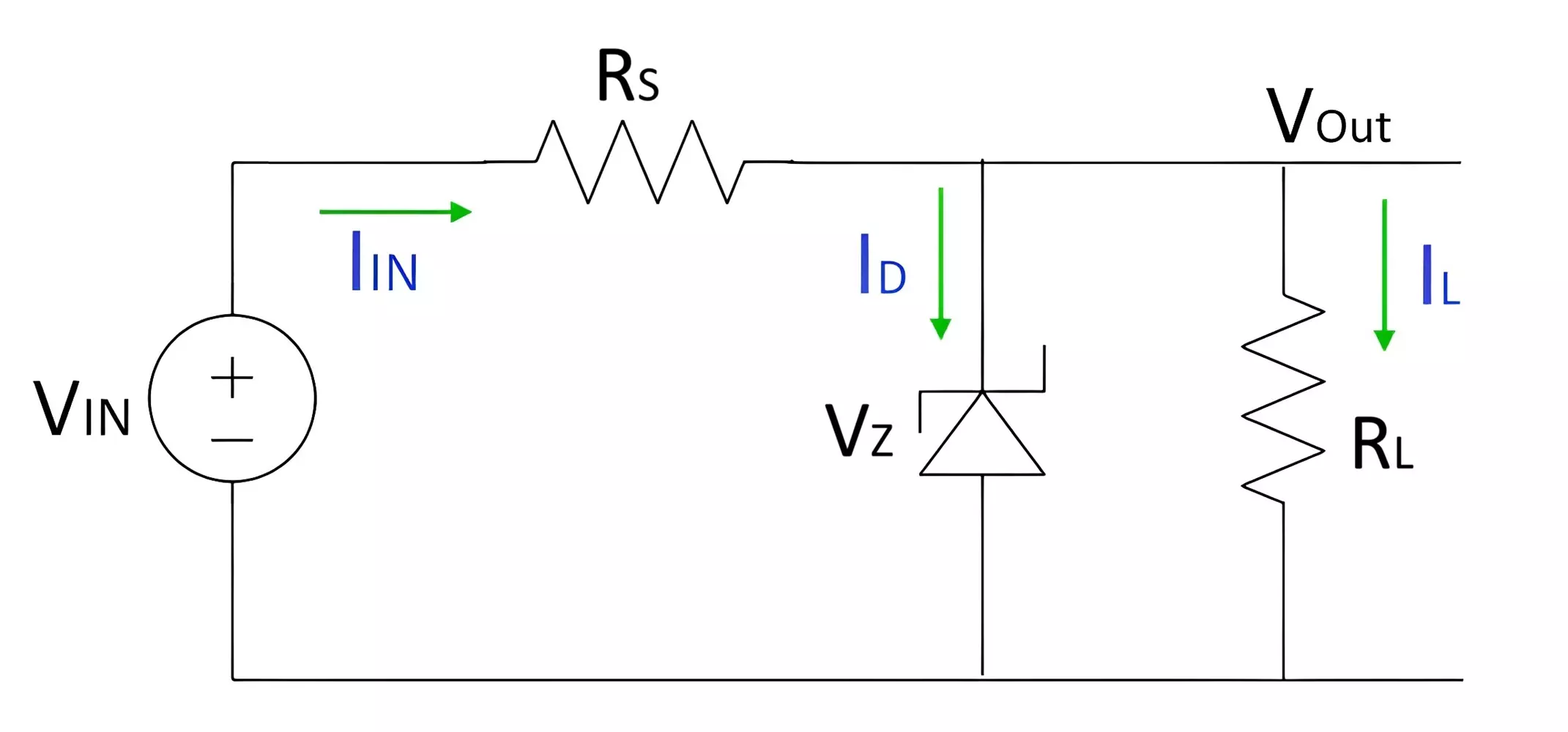
When operated in its reverse breakdown region, the voltage across the Zener diode remains almost constant and equal to its Zener voltage (VZ). By connecting a suitable current-limiting resistor in series with the diode, a stable output voltage can be obtained across the load.
The basic voltage regulator circuit consists of:
- Input DC supply voltage (VIN)
- Series current-limiting resistor (RS)
- Zener diode connected in reverse bias
- Load resistance (RL)
The Zener diode is connected in parallel with the load so that the regulated output voltage appears across both the load and the diode.
Working of Zener Voltage Regulator
When the input voltage exceeds the Zener voltage:
- The Zener diode enters the reverse breakdown region.
- The voltage across the diode remains approximately constant.
- The same constant voltage appears across the load.
- Changes in input voltage are absorbed as changes in Zener current.
- The output voltage remains stable.
Output Voltage:
VOUT ≈ VZ
- VOUT = Regulated output voltage
- VZ = Zener breakdown voltage
Current Relationships:
IS = IZ + IL
- IS = Current through series resistor
- IZ = Zener current
- IL = Load current
The current through the series resistor is given by:
IS = (VIN – VZ) / RS
Design Conditions for Proper Regulation
IZK ≤ IZ ≤ IZM
- IZK = Minimum Zener current (knee current)
- IZM = Maximum Zener current
If the Zener current falls below IZK, regulation is lost.
If the Zener current exceeds IZM, the diode may be damaged.
Operation During Input Voltage Variations
- When Input Voltage Increases
- The current through the series resistor increases.
- The excess current flows through the Zener diode.
- The Zener current increases.
- The output voltage remains approximately constant.
- When Input Voltage Decreases
- The current through the series resistor decreases.
- The Zener current decreases.
- The output voltage remains constant as long as the diode stays in breakdown.
Operation During Load Variations
- When Load Current Increases
- Load current increases.
- Zener current decreases.
- Total current through the resistor remains nearly unchanged.
- The output voltage remains regulated.
- When Load Current Decreases
- Zener current increases.
- The Zener diode absorbs the excess current.
- The output voltage remains constant.
This automatic current adjustment is the reason why a Zener diode can regulate voltage effectively.
Practical Design Examples
Example 1: Design a 5 V regulated power supply using a Zener diode with the following specifications:
- Input Voltage (VIN) = 12 V
- Zener Voltage (VZ) = 5.1 V
- Load Current (IL) = 20 mA
- Minimum Zener Current (IZ(min)) = 5 mA
Total Required Current:
IS = IL + IZ(min)
IS = 20 mA + 5 mA = 25 mA
Series Resistor:
RS = (VIN – VZ) / IS
RS = (12 – 5.1)/0.025 = 276 Ω
The nearest standard value is 270 Ω
Output Voltage:
VOUT ≈ VZ = 5.1 V
Final Design Values:
- Zener Diode = 5.1 V
- Series Resistor = 270 Ω
- Output Voltage = 5.1 V
- Load Current = 20 mA
Example 2: Determine the maximum safe current for a 12 V, 1 W Zener diode.
- Zener Voltage (VZ) = 12 V
- Power Rating (PD(max)) = 1 W
Maximum Safe Current:
IZM = PD(max) / VZ
IZM = 1/12 = 0.0833 A = 83.3 mA
The maximum safe Zener current IZM ≈ 83 mA
Any current above this value may exceed the power rating and damage the diode.
Advantages of Zener Diode
The Zener diode is one of the most widely used semiconductor devices because of its simplicity, reliability, and excellent voltage regulation characteristics. It offers several advantages in power supply, protection, and reference voltage applications.
- Excellent Voltage Regulation: Maintains a nearly constant output voltage over a wide range of input voltage and load current variations.
- Simple Circuit Design: Requires only a Zener diode and a series resistor to implement a basic voltage regulator.
- Low Cost: Zener diodes are inexpensive and readily available in a wide range of voltage ratings.
- Fast Response: Responds quickly to changes in voltage, making it suitable for protection and regulation applications.
- High Reliability: Can operate continuously in the reverse breakdown region without degradation when used within specified ratings.
- Wide Voltage Range: Available with breakdown voltages ranging from approximately 2.4 V to over 200 V.
- Compact Size: Requires very little board space and is available in both through-hole and surface-mount packages.
- Low Maintenance: Does not require adjustment or calibration after installation.
Disadvantages of Zener Diode
Despite its many advantages, the Zener diode has certain limitations that restrict its use in high-power and high-efficiency applications.
- Low Efficiency: A significant amount of power is dissipated in the Zener diode and series resistor.
- Limited Current Capability: Not suitable for supplying large load currents without additional circuitry.
- Power Dissipation Issues: Excessive current can cause overheating and damage the device.
- Output Voltage Variation: The output voltage changes slightly due to dynamic resistance.
- Temperature Dependency: The breakdown voltage may vary with temperature.
- Limited Regulation Accuracy: Precision voltage references often require specialized reference ICs instead of standard Zener diodes.
- Not Suitable for High-Power Regulation: Large currents require power transistors or switching regulators.
Applications of Zener Diode
Due to its unique reverse breakdown characteristics, the Zener diode is used extensively in electronic circuits for voltage regulation, protection, and waveform shaping applications.
- Voltage Regulation:
- Used as a shunt voltage regulator.
- Maintains a constant output voltage despite supply fluctuations.
- Widely used in low-power regulated power supplies.
- Voltage Reference Circuits:
- Overvoltage Protection:
- Protects electronic circuits from excessive voltage.
- Limits voltage to a safe value during abnormal conditions.
- Used in power supply protection circuits.
- Clipping Circuits:
- Used to remove unwanted portions of a waveform.
- Limits signal amplitude to predetermined levels.
- Commonly used in communication and signal processing circuits.
- Clamping Circuits:
- Used to shift the DC level of an AC waveform.
- Prevents signal voltages from exceeding safe operating limits.
- Meter Protection:
- Protects sensitive measuring instruments from accidental overvoltage.
- Used in voltmeters, multimeters, and instrumentation equipment.
- Surge Protection Circuits:
- Protects circuits from transient voltage spikes.
- Used in conjunction with TVS diodes and MOVs.
- Switching Circuits:
- Used as voltage threshold detectors.
- Provides controlled switching action at specific voltages.
- Bias Stabilization Circuits:
- Maintains stable transistor operating points.
- Improves amplifier stability.
- Power Supply Circuits:
- Used in linear power supplies.
- Provides regulated voltages for low-power electronic systems.
- Protection of Microcontrollers and ICs:
- Protects GPIO pins and sensitive IC inputs.
- Prevents damage due to excessive voltage levels.
- SMPS Feedback Circuits:
- Programmable Zener devices such as TL431 are extensively used in switched-mode power supplies.
- Provide accurate output voltage regulation.
Zener Diode vs PN Junction Diode vs TVS Diode
Although all three devices are based on a PN junction, their construction, operating characteristics, and applications differ significantly.
| Parameter | Zener Diode | PN Junction Diode | TVS Diode |
|---|---|---|---|
| Primary Purpose | Voltage regulation and voltage reference | Rectification and switching | Transient voltage protection |
| Normal Operating Region | Reverse breakdown region | Forward bias region | Reverse breakdown during surges |
| Reverse Breakdown Operation | Designed for continuous operation | Normally avoided | Designed for short-duration surges |
| Voltage Regulation | Excellent | Not suitable | Not intended for regulation |
| Response Time | Fast | Moderate | Extremely fast (picoseconds to nanoseconds) |
| Current Handling During Breakdown | Moderate | May be damaged | Very high surge current capability |
| Power Dissipation Capability | Low to moderate | Low to moderate | Very high during transient events |
| Junction Area | Moderate | Small | Large |
| Main Application | Voltage regulators | Rectifiers and switching circuits | ESD and surge protection |
| Typical Breakdown Voltage Range | 2.4 V to 200 V+ | Not specified for operation | 5 V to several hundred volts |
| Continuous Breakdown Operation | Yes | No | No, only during transient events |
| Examples | 1N4733A, BZX55, BZX79 | 1N4007, 1N4148 | SMBJ5.0A, P6KE Series |
- Zener Diode: Primarily used for voltage regulation and voltage reference applications.
- PN Junction Diode: Primarily used for rectification, switching, and signal processing.
- TVS Diode: Primarily used for protecting electronic circuits against ESD, lightning, and transient overvoltage events.
- A Zener diode can operate continuously in reverse breakdown, whereas a TVS diode is intended to conduct only during transient events.
- TVS diodes can handle significantly higher surge currents than standard Zener diodes.
Conclusion
The Zener diode is an important semiconductor device used for voltage regulation, voltage reference generation, overvoltage protection, and waveform shaping. Unlike a conventional PN junction diode, it is designed to operate safely in the reverse breakdown region, maintaining a nearly constant voltage over a wide range of currents.
Its ability to provide stable voltage makes it widely used in power supplies, analog circuits, instrumentation, communication systems, and embedded electronics. Depending on its breakdown voltage, it may operate through Zener breakdown, avalanche breakdown, or both.
In this article, we discussed the symbol, construction, working principle, V-I characteristics, breakdown mechanisms, specifications, applications, advantages, disadvantages, and practical uses of Zener diodes. Understanding these concepts helps in selecting the right Zener diode for electronic circuit design.
Despite the availability of advanced voltage regulators, Zener diodes remain popular due to their simplicity, low cost, compact size, and reliability. They continue to be widely used as voltage regulators, references, clipping devices, and protection components in electronic circuits.
Frequently Asked Questions (FAQ)
What is a Zener diode?
A Zener diode is a semiconductor diode designed to operate in reverse breakdown and maintain a nearly constant voltage.
Why is a Zener diode operated in reverse bias?
Its voltage regulation property appears in the reverse breakdown region.
What is Zener voltage (VZ)?
The reverse breakdown voltage at which the Zener diode begins conducting and regulates voltage.
What is the difference between a Zener diode and a normal diode?
A normal diode is used mainly in forward bias, while a Zener diode is designed to operate safely in reverse breakdown.
What is the typical voltage range of Zener diodes?
Commercial Zener diodes are available from about 2.4 V to over 200 V.
What is Zener breakdown?
A low-voltage breakdown mechanism caused by a strong electric field in a heavily doped PN junction.
What is avalanche breakdown?
A high-voltage breakdown mechanism caused by impact ionization in a lightly doped PN junction.
What is the difference between Zener and avalanche breakdown?
Zener breakdown occurs at lower voltages, while avalanche breakdown occurs at higher voltages.
Why is a series resistor used with a Zener diode?
To limit current and protect the diode from excessive power dissipation.
What is the power dissipation formula of a Zener diode?
PZ = VZ × IZ
What are the common applications of Zener diodes?
Voltage regulation, voltage reference circuits, overvoltage protection, clipping, clamping, and IC protection.
What is the difference between a Zener diode and a TVS diode?
A Zener diode is mainly used for voltage regulation, whereas a TVS diode is designed for transient surge protection.
How do I choose the correct Zener diode?
Consider the required Zener voltage, power rating, current rating, tolerance, and application requirements.
Types of Diodes: Symbol, Working, Characteristics and Applications
Light Emitting Diode LED – Symbol, Construction, Working, Types and Applications
Laser Diode – Symbol, Construction, Working, Types and Applications
Rectifier Circuit: Construction, Working, Types and Applications
Diode Clamper Circuit Diagram, Types, Working and Applications
Diode Clipper Circuit Diagram, Types, Working and Applications
