Diode is a versatile electronic component, many specialized types of diodes exist, each optimized for specific applications such as voltage regulation, light emission, high-speed switching, and detection.
It is one of the most fundamental semiconductor devices used in electronics. It plays a critical role in controlling the direction of current flow in a circuit. From simple rectification in power supplies to high-speed switching and signal modulation, diodes form the backbone of both analog and digital electronic systems.
At its core, a diode is a two-terminal nonlinear device constructed using semiconductor materials such as silicon or germanium. Its operation is based on the behavior of charge carriers (electrons and holes) across a P-N junction, which creates a unique property, unidirectional conduction.
Diodes are widely used in:
- Power supply rectifiers (AC to DC conversion)
- Signal clipping and clamping circuits
- Voltage regulation
- Switching and protection circuits
- Communication systems
Definition of Diode
A diode is a two-terminal semiconductor device that allows electric current to flow primarily in one direction (forward bias) and blocks it in the opposite direction (reverse bias).
- When the diode is forward biased (positive voltage applied to P-side and negative to N-side), it conducts current after overcoming the barrier potential.
- When reverse biased, it ideally blocks current except for a very small leakage current.
This unidirectional property makes the diode function similar to an electronic one-way valve for current.
Symbol of Diode
The circuit symbol of a diode represents its directional behavior.

- Symbol Explanation:
- The triangle/arrow side represents the Anode (P-type region)
- The vertical line/bar represents the Cathode (N-type region)
- Current flows from Anode → Cathode in forward bias
- The bar (cathode) acts as a blocking side for reverse current
- In real components:
- The cathode is usually marked with a band/stripe
- The opposite terminal is the anode

Working of Diode
The operation of a diode is governed by the behavior of charge carriers at the PN junction, particularly the formation and control of the depletion region and potential barrier. Depending on the applied external voltage, a diode operates in three primary modes:
Unbiased Condition (No External Voltage)
When no external voltage is applied:
- Electrons from the N-region diffuse into the P-region and recombine with holes
- Holes from the P-region diffuse into the N-region
- This diffusion creates a depletion region (region devoid of free carriers)
- An internal electric field develops, forming a barrier potential

Barrier Potential (Typical Values):
- Silicon diode ≈ 0.7 V
- Germanium diode ≈ 0.3 V
- At equilibrium:
- Diffusion current = Drift current
- Net current = Zero
Forward Bias Operation
Condition: P-side connected to positive terminal, N-side to negative terminal
What happens physically:
- External voltage reduces the barrier potential
- Depletion region narrows
- Majority carriers gain enough energy to cross the junction:
- Electrons move from N → P
- Holes move from P → N
- Recombination occurs near the junction
- Once the applied voltage exceeds the cut-off (threshold) voltage, current increases rapidly (exponentially)

Current Behavior:
The diode current approximately follows the exponential law:
I = Is (eV / ηVt) − 1)
- I = diode current
- Is = reverse saturation current
- V = applied voltage
- Vt = thermal voltage (~26 mV at room temperature)
- η = emission coefficient (≈1 for Ge, ≈2 for Si)
Key Insight:
A small increase in forward voltage results in a large increase in current, making the diode highly nonlinear.
Reverse Bias Operation
Condition: P-side connected to negative terminal, N-side to positive terminal
What happens physically:
- External voltage increases the barrier potential
- Depletion region widens
- Majority carriers are pulled away from the junction
- Only minority carriers contribute to current
- Very small current flows called reverse saturation current (Iₛ)
- This current is temperature dependent

Breakdown Region
If reverse voltage is increased beyond a critical value:
- The diode enters breakdown region
- Current increases sharply
Two mechanisms:
- Zener Breakdown (low voltage, heavily doped junction)
- Avalanche Breakdown (high voltage, lightly doped junction)
In a normal diode avalanche breakdown can damage the device unless current is limited.
Summary of Working
| Bias Condition | Depletion Region | Current Flow | Behavior |
|---|---|---|---|
| Zero Bias | Formed | No net current | Equilibrium |
| Forward Bias | Narrows | High current | Conduction |
| Reverse Bias | Widens | Very small current | Blocking |
| Breakdown | Collapses | Very high current | Dangerous (if uncontrolled) |
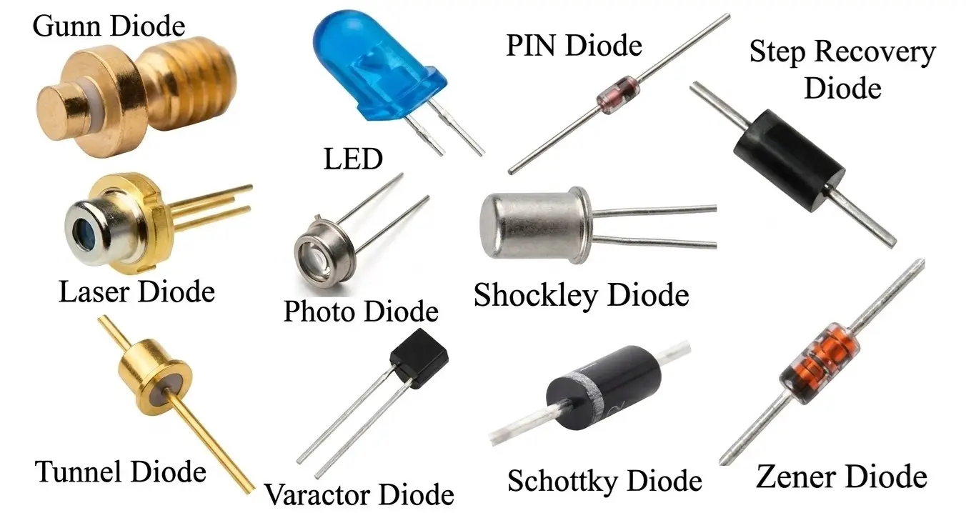
Classification of Diodes
A diode is not a single device category; it is a family of semiconductor junction devices engineered for different electrical behaviors. The classification is best understood based on function, construction, and physical operating principle.
Below is a complete and structured classification suitable for a technical article.
By Construction (Junction Type)
- PN Junction Diode
- Standard diode formed by joining P-type and N-type semiconductor
- Most fundamental type
- Used in rectification, clipping, and switching
- PIN Diode
- Structure: P–Intrinsic–N
- Intrinsic layer increases depletion width
- Offers low capacitance and high-frequency performance
- Used in RF switches and attenuators
- Schottky Diode
- Metal–semiconductor junction (no P-N junction)
- Very low forward voltage (~0.2–0.3 V)
- Extremely fast switching
- Used in SMPS, high-speed circuits
By Function / Application
- Rectifier Diodes (Power Diodes)
- Designed for high current and voltage
- Used in half-wave/full-wave rectifiers and power supplies
- Types: General purpose, Fast recovery, Ultra-fast recovery
- Zener Diode
- Operates in reverse breakdown region
- Maintains constant voltage
- Used for voltage regulation and reference circuits
- Light Emitting Diode (LED)
- Emits light when forward biased
- Based on electroluminescence
- Used in: Indicators, Displays and Lighting
- Laser Diode
- Produces coherent light (laser beam)
- High intensity and narrow wavelength
- Used in: Optical communication and CD/DVD drives
- Photodiode
- Converts light into electrical current
- Operates mainly in reverse bias
- Used in: Sensors and Optical receivers
- Solar Cell (Photovoltaic Diode)
- Converts light into electrical energy
- Essentially a large-area photodiode
- Used in: Solar panels and Renewable energy systems
- Varicap/Varactor Diode
- Works as a voltage-controlled capacitor
- Capacitance varies with reverse voltage
- Used in: Tuners and RF oscillators
- Tunnel Diode
- Heavily doped junction
- Shows negative resistance region
- Used in: High-speed switching and Microwave oscillators
- Avalanche Diode
- Designed to operate in avalanche breakdown region
- Used for: Voltage protection and Noise generation
- TVS Diode (Transient Voltage Suppression)
- Protects circuits from voltage spikes
- Very fast response
- Used in: ESD protection and Surge suppression
- Step Recovery Diode
- Also called snap-off diode
- Produces sharp pulses
- Used in: Frequency multipliers and Pulse shaping
- Gunn Diode (Not a true PN diode)
- No P-N junction
- Works on transferred electron effect
- Used in: Microwave oscillators and Radar systems
Based on Switching Speed
- General Purpose Diodes
- Slow switching
- Used in low-frequency applications
- Fast Switching Diodes
- Reduced reverse recovery time
- Used in digital and switching circuits
- Ultra-Fast / High-Speed Diodes
- Very low recovery time
- Used in SMPS and RF systems
Based on Material Used
- Silicon Diodes
- Most widely used
- Higher thermal stability
- Forward drop ≈ 0.7 V
- Germanium Diodes
- Lower forward drop (~0.3 V)
- Higher leakage current
- Used in low-voltage applications
- Gallium Arsenide (GaAs) Diodes
- Used in high-frequency and optoelectronic devices
- Found in LEDs, laser diodes
By Special Characteristics
- Constant Current Diode
- Maintains constant current over voltage range
- Shockley Diode
- Four-layer device (PNPN)
- Acts as a switch
- Backward Diode
- Conducts better in reverse direction (low voltage)
- Used in RF detection
Classification Summary
| Category | Key Types |
|---|---|
| Construction | PN, PIN, Schottky |
| Function | Zener, LED, Photodiode, Varactor, Tunnel, TVS, etc. |
| Speed | General, Fast, Ultra-fast |
| Material | Silicon, Germanium, GaAs |
| Special | Gunn, Step recovery, Shockley |
Types of Diodes in Detail
Let’s explore all the types of diodes in detail with their symbol, construction, working, characteristics and applications.
PN Junction Diode
The PN junction diode is the most fundamental and widely used semiconductor diode. It serves as the base model from which all other specialized diodes are derived.

Symbol
- Represented by a triangle pointing toward a vertical line
- Anode (P-side) → Triangle side
- Cathode (N-side) → Vertical line
- Indicates direction of conventional current flow (Anode → Cathode)
Construction
A PN junction diode is formed by joining two differently doped semiconductor regions:
- P-type region
- Doped with trivalent impurities (e.g., Boron)
- Majority carriers → Holes
- N-type region
- Doped with pentavalent impurities (e.g., Phosphorus)
- Majority carriers → Electrons
- At the junction, a depletion region is formed due to recombination of electrons and holes
- This region is free of mobile charge carriers and acts as an insulating barrier
- A built-in electric field creates a potential barrier (~0.7 V for Si, ~0.3 V for Ge)
Working Principle
The operation depends on biasing conditions:
- Forward Bias
- P-side → Positive, N-side → Negative
- Barrier potential reduces
- Depletion region narrows
- Majority carriers cross the junction
- Diode conducts heavily after cut-in voltage
- Reverse Bias
- P-side → Negative, N-side → Positive
- Barrier potential increases
- Depletion region widens
- Only minor leakage current flows
- Breakdown (High Reverse Voltage)
- Sudden increase in current
- Can occur via:
- Avalanche effect
- Zener effect (in special cases)
VI Characteristics
- Forward Region
- Current rises exponentially after threshold voltage
- Silicon: ~0.7 V, Germanium: ~0.3 V
- Reverse Region
- Very small current (reverse saturation current Iₛ)
- Nearly constant until breakdown
- Breakdown Region
- Sharp increase in current
- Must be externally limited
Characteristics
- Unidirectional conduction
- Nonlinear device (exponential response)
- Temperature-dependent behavior
- Forward resistance low, reverse resistance very high
Applications
- Rectifiers (AC to DC conversion)
- Signal clipping and clamping circuits
- Switching applications
- Protection circuits (freewheeling diode)
- Demodulation (AM detection)
PIN Diode
The PIN diode is a modified P–N junction diode that includes an intrinsic (undoped) semiconductor layer between the P and N regions. This structure significantly alters its electrical behavior, making it highly useful in high-frequency and RF applications.

Symbol
- Similar to a standard diode symbol
- Sometimes annotated to indicate the intrinsic (I) layer
- Terminals: Anode (P-region), Cathode (N-region)
Construction
The PIN diode consists of three layers:
- P-type region (heavily doped)
- Intrinsic region (I-layer)
- Very lightly doped or nearly pure semiconductor
- Much wider depletion region compared to normal diode
- N-type region (heavily doped)
Key Structural Advantage:
The intrinsic layer increases junction width, resulting in:
- Low junction capacitance
- High breakdown voltage
- Better high-frequency performance
Working Principle
- Forward Bias
- External voltage reduces barrier
- Charge carriers are injected into the intrinsic region
- The I-layer gets filled with electrons and holes (charge storage)
- Device behaves like a variable resistor
- Resistance decreases as forward current increases
- Reverse Bias
- Depletion region expands across the intrinsic layer
- Very few charge carriers present
- Acts like a capacitor with very low capacitance
- Offers high resistance (almost open circuit)
VI Characteristics
- Similar exponential behavior as PN diode
- Due to intrinsic layer:
- Slower switching (charge storage)
- More stable at high frequencies
Characteristics
- Wide depletion region
- Low junction capacitance
- High reverse breakdown voltage
- Acts as:
- Resistor (forward bias)
- Capacitor (reverse bias)
- Excellent for RF and microwave frequencies
Applications
- RF switches
- Microwave attenuators
- RF modulators and demodulators
- Phase shifters
- High-frequency signal control circuits
Schottky Diode
The Schottky diode is a high-speed semiconductor diode formed by a metal–semiconductor junction instead of a conventional P–N junction. It is widely used where low forward voltage drop and fast switching are critical.

Symbol
- Similar to a standard diode symbol
- Cathode side often drawn with a bent or stylized line to distinguish it
- Terminals:
- Anode → Metal side
- Cathode → Semiconductor (usually N-type)
Construction
A Schottky diode is formed by directly contacting:
- Metal layer (e.g., Aluminum, Platinum, Tungsten)
- N-type semiconductor (typically silicon)
- No P-type region → No P–N junction
- Junction formed is called a Schottky barrier
This eliminates minority carrier involvement and makes it a majority carrier device
Working Principle
- Forward Bias
- Metal becomes positive relative to semiconductor
- Barrier height reduces
- Electrons (majority carriers) move from semiconductor → metal
- Conduction occurs with very low voltage drop (~0.2–0.3 V)
- Faster response since no recombination delay
- Reverse Bias
- Barrier height increases
- Electron flow is restricted
- Small reverse current flows (higher than PN diode)
- No charge storage → very fast switching
VI Characteristics
- Forward Region
- Lower cut-in voltage (~0.2–0.3 V)
- Rapid current increase
- Reverse Region
- Higher leakage current than P–N diode
- Lower breakdown voltage (typically)
Characteristics
- Very low forward voltage drop
- Ultra-fast switching speed (no reverse recovery)
- Majority carrier device
- Higher reverse leakage current
- Lower reverse voltage rating compared to PN diodes
Applications
- Switch Mode Power Supplies (SMPS)
- Efficient power conversion (reduced losses)
- High-frequency rectification (>100 kHz)
- Freewheeling / flyback diodes
- Clamping and protection circuits
- OR-ing diodes in power systems
Power Diode (Rectifier Diode)
A Power Diode is a PN junction diode specifically engineered to handle high current and high voltage levels. Unlike small-signal diodes, it is optimized for power conversion applications, especially in rectifiers and switching power supplies.

Symbol
- Same as a standard PN junction diode
- No special symbol difference
- Terminals: Anode (P-side), Cathode (N-side)
Construction
Power diodes are designed with structural modifications to withstand high electrical stress:
- Large junction area → Handles high current
- Thicker depletion region → Supports high reverse voltage
- Often includes a drift region (lightly doped layer)
- Packaged with:
- Metal casing
- Heat dissipation structures (stud mount / bolt type / module)
- Design Focus:
- Thermal management
- High breakdown voltage capability
- Low forward conduction loss
Working Principle
The working is similar to a PN diode but under high-power conditions:
- Forward Bias
- Conducts large current after threshold voltage (~0.7–1 V for silicon)
- Power loss = (Vₓ × I) → generates heat
- Requires heat sinking
- Reverse Bias
- Blocks high voltage
- Only small leakage current flows
- Reverse Recovery (Important)
- When switching from forward to reverse bias:
- Stored charge must be removed
- Causes reverse recovery current
- This affects: Switching speed, Power loss and Efficiency
- When switching from forward to reverse bias:
VI Characteristics
- Similar exponential forward region
- Higher current handling capability
- Reverse region supports high voltage blocking
- Breakdown occurs at much higher voltages
Types of Power Diodes
- General Purpose Diodes
- Slow switching (high reverse recovery time)
- Used in 50–60 Hz rectifiers
- Fast Recovery Diodes
- Reduced reverse recovery time
- Used in high-frequency circuits
- Ultra-Fast Diodes
- Very low recovery time
- Used in: SMPS and Inverters
Characteristics
- High current rating (A to kA range)
- High voltage rating (100 V to several kV)
- Significant heat generation
- Reverse recovery is a critical parameter
- Efficiency depends on switching speed and losses
Applications
- AC to DC Rectifiers (Power Supplies)
- Bridge rectifier circuits
- Freewheeling diodes in inductive loads
- SMPS and inverters
- Battery charging circuits
Zener Diode
The Zener diode is a specially designed P–N junction diode that is intended to operate in the reverse breakdown region. Unlike a normal diode (which gets damaged in breakdown), a Zener diode safely utilizes this region to provide stable and regulated voltage.

Symbol
- Similar to a standard diode
- Cathode line is bent or zig-zag shaped, indicating Zener behavior
- Terminals: Anode (P-side), Cathode (N-side)
Construction
- Fabricated using a heavily doped PN junction
- Heavy doping results in:
- Thin depletion region
- Precisely controlled breakdown voltage
- Breakdown voltage (Zener voltage, VZ) is predefined during manufacturing
- Can range from a few volts to hundreds of volts
Working Principle
- Forward Bias
- Acts like a normal diode
- Conducts after ~0.7 V (for silicon)
- Reverse Bias (Main Operation)
- Initially behaves like a normal diode (small leakage current)
- When reverse voltage reaches Zener voltage (VZ) breakdown occurs
- Mechanisms:
- Zener Breakdown (Low Voltage < 5–6 V)
- Strong electric field pulls electrons across junction
- Quantum tunneling effect
- Avalanche Breakdown (High Voltage > 6 V)
- Charge carriers gain high energy
- Cause impact ionization
- Zener Breakdown (Low Voltage < 5–6 V)
- After breakdown:
- Voltage across diode remains almost constant
- Current increases rapidly
- Requires series resistor to limit current
VI Characteristics
- V ≈ VZ (in breakdown region)
- Forward Region
- Same as normal diode
- Reverse Region
- Small leakage current until breakdown
- Breakdown Region
- Voltage remains nearly constant at V_Z
- Current increases sharply
Characteristics
- Operates safely in reverse breakdown
- Provides constant output voltage
- Sharp breakdown characteristic
- Temperature-dependent behavior:
- Zener effect → negative coefficient
- Avalanche → positive coefficient
Applications
- Voltage regulation (most important use)
- Voltage reference circuits
- Overvoltage protection
- Clipping and clamping circuits
- Meter protection circuits
Light Emitting Diode (LED)
The Light Emitting Diode (LED) is a semiconductor diode that emits visible or invisible light when it is forward biased. Unlike standard diodes that dissipate energy as heat, an LED converts electrical energy into optical energy through the process of electroluminescence.

Symbol
- Similar to a standard diode symbol
- Includes two outward arrows, indicating light emission
- Terminals: Anode (P-side), Cathode (N-side)
Construction
An LED is made using compound semiconductor materials instead of pure silicon:
- Common materials:
- Gallium Arsenide (GaAs)
- Gallium Phosphide (GaP)
- Gallium Arsenide Phosphide (GaAsP)
- Gallium Nitride (GaN)
- P-type and N-type layers form a junction
- Enclosed in a transparent epoxy lens
- The lens acts as protection and light focusing element
- The material determines the color (wavelength) of emitted light
Working Principle
- Forward Bias Operation
- When forward biased: Electrons from N-region recombine with holes in P-region
- During recombination: Energy is released in the form of photons (light)
- This phenomenon is called electroluminescence
- Energy Relation: E = hν
- E = energy of photon
- h = Planck’s constant
- ν = frequency of light
- Higher energy → shorter wavelength → different color
- Reverse Bias
- LED behaves like a normal diode
- Does not emit light
- Excess reverse voltage can damage the device
VI Characteristics
- Forward Region
- Conducts after threshold voltage (varies with color):
- Red: ~1.8–2.2 V
- Green: ~2–3 V
- Blue/White: ~3–3.6 V
- Conducts after threshold voltage (varies with color):
- Reverse Region
- Very low tolerance for reverse voltage
- Less than 5V
Characteristics
- Emits light in forward bias
- Color depends on semiconductor material
- Low power consumption
- Fast switching speed
- Long operational life
- Highly efficient compared to incandescent sources
Applications
- Indicator lights (power, status signals)
- Display systems (7-segment, dot matrix)
- Lighting (LED bulbs, streetlights)
- Optical communication systems
- Remote controls (IR LEDs)
Laser Diode
A Laser Diode is a specialized semiconductor diode that emits coherent, monochromatic, and highly directional light through the process of stimulated emission. Unlike LEDs (which emit incoherent light), a laser diode produces a focused beam with very narrow wavelength spread.

Symbol
- Based on the LED symbol
- Includes outward arrows indicating light emission
- Often annotated to represent laser action
- Terminals: Anode (P-side), Cathode (N-side)
Construction
- Made using compound semiconductor materials (e.g., GaAs, InP)
- Structure includes:
- P–N junction
- Active region (where light is generated)
- Optical cavity formed by reflective surfaces
- Presence of optical resonant cavity for light amplification
- Ends of the diode act as mirrors to reflect photons
Working Principle
- Forward Bias Operation
- Electrons recombine with holes in the active region
- Initially produces spontaneous emission
- When current exceeds a threshold level:
- Stimulated emission dominates
- Photons trigger more photon generation
- Produces coherent, intense, and directional laser beam
- Reverse Bias
- Acts like a normal diode
- No light emission
VI Characteristics
- Popt ∝ (I−Ith)
- Similar to LED but with a threshold current
- Below threshold: Weak light emission
- Above threshold: Sudden increase in light intensity (laser action)
Characteristics
- Emits coherent light
- Very narrow wavelength (monochromatic)
- Highly directional beam
- Requires precise current control
- Sensitive to temperature and overheating
Applications
- Optical communication (fiber optics)
- CD/DVD/Blu-ray drives
- Laser printers
- Barcode scanners
- Medical and industrial lasers
Photodiode
A Photodiode is a semiconductor diode that converts incident light into electrical current. It operates primarily in reverse bias, where it acts as a light-controlled current source. Unlike LEDs (which emit light), a photodiode performs the opposite function light detection.

Symbol
- Similar to a standard diode symbol
- Includes two arrows pointing toward the junction, indicating incoming light
- Terminals: Anode (P-side), Cathode (N-side)
Construction
A photodiode is typically made from silicon or other photosensitive semiconductor materials and designed to efficiently capture light.
- PN junction (or PIN structure for better performance)
- Transparent window or lens allows light to reach the junction
- Often optimized for:
- Maximum light absorption
- Fast response
- Large depletion region improves light sensitivity and speed
Working Principle
- Reverse Bias Operation (Main Mode)
- Photodiode is operated in reverse bias
- Depletion region becomes wide
- When light (photons) falls on the junction:
-
- Photons generate electron–hole pairs
- Internal electric field separates these carriers:
- Electrons → N-side
- Holes → P-side
-
- This creates a photocurrent
- Current Relation: I = Id + Iph
- Id = dark current (no light)
- Iph = photocurrent (due to light)
- Photocurrent is directly proportional to light intensity
- Zero Bias (Photovoltaic Mode)
- Operates without external voltage
- Generates small voltage (like a solar cell)
- Slower but low noise
VI Characteristics
- In darkness: Only small dark current flows
- Under illumination:
- Reverse current increases significantly
- Shift in IV curve proportional to light intensity
- Very fast response due to:
- Minimal charge storage
- Wide depletion region
Characteristics
- Converts light → electrical signal
- Operates mainly in reverse bias
- High sensitivity to light
- Fast switching speed
- Low noise (in proper biasing)
- Output current proportional to illumination
Applications
- Light sensors
- Optical communication receivers
- IR detection systems
- Smoke detectors
- Automatic lighting systems
- Encoders and position sensors
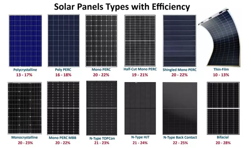
Solar Cell (Photovoltaic Diode)
A Solar Cell (or Photovoltaic Diode) is a semiconductor device that converts light energy directly into electrical energy using the photovoltaic effect. Electrically, it behaves like a photodiode operated in zero-bias (photovoltaic) mode, but optimized for power generation rather than sensing.
Symbol
- Similar to a photodiode symbol
- Arrows directed toward the junction (incoming light)
- Sometimes enclosed in a box to represent a cell/module
- Terminals: Positive (P-side), Negative (N-side)
Construction
A solar cell is typically fabricated from silicon semiconductor material:
- P-type layer (base)
- N-type layer (emitter) forming a P–N junction
- Front metal grid → collects electrons (minimizes shading)
- Back metal contact → completes the circuit
- Anti-reflective coating → increases light absorption
- Encapsulated in protective material (glass/polymer)
- Large surface area for maximum light absorption
- Optimized junction depth for efficient carrier collection
Working Principle (Photovoltaic Effect)
- Light Absorption
- Incident photons strike the semiconductor
- If photon energy ≥ bandgap: Electron–hole pairs are generated
- Charge Separation
- Built-in electric field at the junction separates carriers:
- Electrons → N-side
- Holes → P-side
- This produces: DC current and voltage
- When an external circuit is connected electrons flow through the load
- Built-in electric field at the junction separates carriers:
Current Equation
I = Iph − Is (eV / ηVt) − 1)
- Iph = photocurrent (depends on light intensity)
- Is = saturation current
Output current decreases as voltage increases (nonlinear behavior)
VI Characteristics
- Short-Circuit Current (Isc): Maximum current when voltage = 0
- Open-Circuit Voltage (Voc): Maximum voltage when current = 0
- Maximum Power Point (MPP): Point where (V × I) is maximum
The IV curve shifts with: Light intensity and Temperature
Characteristics
- Generates electricity without external bias
- Output depends on:
- Light intensity
- Temperature
- Efficiency typically 15%–25% (silicon cells)
- No moving parts → high reliability
- Environmentally friendly energy source
- Series and parallel combination → forms solar modules
Applications
- Solar panels (rooftop systems)
- Solar power plants
- Calculators and small electronics
- Battery charging systems
- Space satellites and remote systems
Varactor (Varicap) Diode
The Varactor diode (also called Varicap diode) is a semiconductor diode designed to operate as a voltage-controlled capacitor. It exploits the property of a reverse-biased P–N junction where the junction capacitance varies with applied voltage.

Symbol
- Similar to a diode symbol
- Includes capacitor plates on one side
- Indicates its function as a variable capacitor
- Terminals: Anode (P-side), Cathode (N-side)
Construction
- Fabricated as a PN junction diode
- Designed with:
- Carefully controlled doping profile
- Optimized junction geometry
- Operated only in reverse bias
- The depletion region acts as dielectric
- P and N regions act as capacitor plates
Working Principle
- Only Reverse Bias Operation
- When reverse voltage is applied:
- Depletion region widens
- Effective distance between plates increases
- Capacitance decreases
Capacitance Relation
Cj ∝ 1 / √VR
- Cj = junction capacitance
- VR = reverse voltage
- Increasing reverse voltage → decreasing capacitance
VI Characteristics
- In reverse bias:
- Very small leakage current
- No conduction (ideal operation region)
- In forward bias: Behaves like a normal diode (not used in this mode)
Characteristics
- Acts as a variable capacitor
- Controlled by reverse voltage
- High Q factor (low loss at RF)
- No mechanical parts → highly reliable
- Fast response
Applications
- RF tuning circuits (radio, TV receivers)
- Voltage Controlled Oscillators (VCOs)
- Frequency modulation (FM circuits)
- Phase-locked loops (PLL)
- Electronic tuning systems
Tunnel Diode
The Tunnel Diode (also known as the Esaki diode, after Leo Esaki) is a heavily doped PN junction diode that exhibits a unique property called negative resistance due to quantum mechanical tunneling.

Symbol
- Similar to a standard diode
- Often includes a modified cathode line indicating special behavior
- Terminals: Anode (P-side), Cathode (N-side)
Construction
- Made by extremely heavy doping of both P and N regions
- This results in:
- Very thin depletion region (≈ 10 nm)
- Overlapping energy bands
- The thin barrier allows electrons to tunnel through the junction instead of overcoming it normally
Working Principle
The operation is based on quantum tunneling, not classical conduction
- Small Forward Bias
- Electrons tunnel directly from N-side to P-side
- Current increases rapidly
- Moderate Forward Bias
- Alignment of energy bands reduces
- Tunneling probability decreases
- Current decreases even though voltage increases
- This region is called the Negative Resistance Region
- High Forward Bias
- Normal diode conduction dominates
- Current increases again
VI Characteristics
- dI/dV < 0 → Negative resistance region
- Peak Point (Ip, Vp) → Maximum tunneling current
- Valley Point (Iv, Vv) → Minimum current
- Between these points current decreases with increasing voltage
Characteristics
- Exhibits negative resistance
- Extremely fast operation
- Works at microwave frequencies
- Low voltage operation
- Sensitive to temperature
Applications
- High-frequency oscillators
- Microwave amplifiers
- Fast switching circuits
- Pulse generators
Avalanche Diode
The Avalanche diode is a PN junction diode specifically designed to operate in the avalanche breakdown region under reverse bias. Unlike ordinary diodes (which can be damaged in breakdown), this device is engineered to safely handle high reverse voltages and large surge currents.

Symbol
- Same as a standard PN junction diode
- No unique symbol distinction in most schematics
- Terminals: Anode (P-side), Cathode (N-side)
Construction
- Fabricated using a lightly doped PN junction
- This results in:
- Wide depletion region
- High breakdown voltage (typically > 6 V)
- Designed to withstand high electric fields without permanent damage
- Optimized for controlled impact ionization
Working Principle
- Reverse Bias Operation: When reverse voltage increases electric field across junction becomes very strong
- Avalanche Breakdown Process:
- Free electrons gain high kinetic energy
- They collide with atoms and generate more electron–hole pairs
- This leads to a chain reaction called impact ionization
- This results in sudden multiplication of carriers and rapid increase in current
VI Characteristics
- In avalanche region I ∝ eαV
- Forward Region: Same as normal diode
- Reverse Region: Small leakage current initially
- Breakdown Region:
- Sharp rise in current at breakdown voltage
- Voltage remains relatively stable
Characteristics
- Operates in high reverse voltage region
- High current handling capability
- Positive temperature coefficient
- Fast response to voltage surges
- Robust compared to normal diodes
Applications
- Voltage surge protection
- Overvoltage protection circuits
- Noise generation circuits
- High-voltage regulation (in some cases)
- Protection in power electronics systems
TVS Diode
A TVS (Transient Voltage Suppression) diode is a protection device designed to clamp high-voltage spikes (transients) and protect sensitive electronic circuits from damage caused by ESD, lightning, or switching surges. It operates by entering avalanche breakdown extremely fast and diverting surge current away from the protected load.

Symbol
- Unidirectional TVS: Similar to a Zener diode symbol
- Bidirectional TVS: Two Zener-like diodes connected back-to-back
- Terminals:
- For unidirectional: Anode & Cathode
- For bidirectional: symmetric terminals
Construction
- Based on a silicon avalanche junction (similar to an avalanche diode)
- Engineered for:
- Very fast response time (picoseconds–nanoseconds)
- High surge current capability
- Available in:
- Unidirectional and bidirectional forms
- Surface-mount (SMT) and axial packages
- Low dynamic resistance → better clamping
- Large junction area → handles high transient energy
Working Principle
- Normal Operation (Standby)
- Under normal voltage:
- TVS diode remains non-conducting
- Only a small leakage current flows
- Transient Event (Surge Condition)
- When voltage exceeds breakdown voltage (VBR):
- Device enters avalanche breakdown
- Conducts heavily
- Diverts surge current to ground
- Limits voltage across the protected circuit
- Clamping Action
- VCL < Vdamage
- VCL = clamping voltage
- Must be lower than the maximum safe voltage of the circuit
- After Surge
- Once transient disappears device returns to high-impedance state
- No permanent damage (if within ratings)
VI Characteristics
- Forward Region: Similar to diode (for unidirectional type)
- Reverse Region: High resistance until breakdown
- Breakdown Region
- Very sharp transition
- Large current with limited voltage rise
Characteristics
- Extremely fast response time
- High peak pulse power capability
- Low clamping voltage
- Available in uni/bidirectional types
- Protects against: ESD, Lightning surges and Inductive switching spikes
Applications
- ESD protection (USB, HDMI, data lines)
- Power supply protection
- Automotive electronics
- Communication equipment
- Industrial control systems
Step Recovery Diode (SRD) / Snap-Off Diode
The Step Recovery Diode (SRD), also called a snap-off diode it is designed to generate extremely fast voltage/current transitions. It exploits a controlled charge storage and abrupt removal mechanism to produce sharp pulses rich in high-frequency harmonics.

Symbol
- Typically drawn similar to a standard diode
- Sometimes annotated as SRD or with a modified cathode marking
- Terminals: Anode (P-side), Cathode (N-side)
Construction
- Based on PN junction with a tailored doping profile, P⁺–N⁻–N⁺ structure
- Key design aspects:
- Controlled carrier lifetime
- Optimized charge storage in the lightly doped region
- Ability to store a significant amount of charge during forward conduction and then remove it abruptly during reverse bias
Working Principle
- Forward Bias (Charge Storage Phase)
- Diode conducts normally
- Excess minority carriers accumulate in the junction and drift region
- The diode behaves like a low-resistance conductor
- Transition to Reverse Bias
- Reverse voltage is applied
- Stored charge does not vanish instantly
- A reverse current flows while removing stored carriers
- Snap-Off (Step Recovery Action)
- Once stored charge is fully depleted current drops abruptly to zero
- This sudden change creates:
- A very sharp current/voltage edge
- Equivalent to a high-frequency pulse
Time-Domain Behavior
- di/dt ≫ 0 (during snap-off transition)
- Extremely high di/dt at the instant of snap-off
- Produces harmonics extending into microwave frequencies
VI Characteristics
- Forward Region: Normal diode conduction with charge storage
- Reverse Region: Reverse current flows briefly (storage removal)
- Snap-Off Point: Sudden current collapse → pulse generation
Characteristics
- Very fast switching (nanosecond range)
- Produces sharp pulses with high harmonic content
- Controlled reverse recovery behavior (intentional and abrupt)
- Suitable for high-frequency operation
Applications
- Frequency multipliers (RF and microwave)
- Pulse generators
- Harmonic generation circuits
- Microwave signal processing
- Sampling circuits
Gunn Diode
The Gunn Diode is a microwave semiconductor device that exhibits negative differential resistance due to the Transferred Electron Effect. Unlike conventional diodes, it is not a PN junction device, it is made from a single N-type semiconductor material.

Symbol
- Represented as a two-terminal device similar to a diode
- No standard PN junction marking
- Terminals: Anode, Cathode
Construction
- Made from N-type semiconductor only
- Common materials:
- Gallium Arsenide (GaAs)
- Indium Phosphide (InP)
- Typically a sandwich structure (N⁺ – N – N⁺)
- No P-region → no junction
- Uses bulk material properties rather than junction behavior
- Designed to support high electric field domains
Working Principle (Transferred Electron Effect)
The operation is based on electron energy band structure, not junction physics
- Low Electric Field
- Electrons move in low-energy conduction band
- High mobility → current increases normally
- High Electric Field (Above Threshold)
- Electrons gain energy and move to a higher energy band
- In this band mobility decreases
- Current decreases even though voltage increases
- Negative Differential Resistance
- dI/dV < 0 (Gunn effect region)
- This region enables oscillation and signal generation
- Domain Formation
- High-field regions called Gunn domains form
- These domains travel across the device
- When they reach the end current pulse is generated
Repetition of this process creates microwave oscillations
VI Characteristics
- Initial region → normal increase in current
- Negative resistance region → current decreases with voltage
- High-field region → stable oscillation
Characteristics
- No PN junction (bulk semiconductor device)
- Exhibits negative differential resistance
- Operates at microwave frequencies (GHz range)
- Requires threshold electric field
- Generates oscillations directly
Applications
- Microwave oscillators
- Radar systems
- Speed detection (radar guns)
- Signal generators (GHz range)
- Automatic door sensors
Constant Current Diode (CCD) / Current Regulator Diode (CRD)
The Constant Current Diode (CCD), also known as a Current Regulator Diode (CRD) is a two-terminal semiconductor device that maintains a nearly constant current over a wide range of applied voltage. Unlike ordinary diodes that regulate voltage, this device is designed to regulate current.

Symbol
- symbol includes a circle with vertical line
- Terminals: Anode, Cathode
Construction
- Typically implemented using a JFET (Junction Field Effect Transistor) internally
- The gate and source are shorted together
- Packaged as a two-terminal device to behave like a diode
- The internal JFET operates in its constant current (saturation) region
Working Principle
- Low Voltage Region
- Device behaves like a resistor
- Current increases with voltage
- Regulation Region (Main Operation)
- After a certain voltage is reached JFET enters pinch-off region
- Current becomes constant and independent of voltage
- This current is called regulated current (I₀)
- Current Behavior
- I ≈ I₀ (constant current region)
- Current remains nearly constant over a wide voltage range
- Small variations may occur due to temperature and device tolerance
VI Characteristics
- Initial Region: Current increases with voltage
- Constant Current Region: Flat curve (current remains constant)
- High Voltage Region: Slight increase due to breakdown effects
Characteristics
- Maintains constant current output
- Wide operating voltage range
- Simple two-terminal device
- No external biasing required
- Temperature-dependent behavior (moderate)
Applications
- LED current limiting
- Constant current sources
- Biasing circuits for transistors
- Current stabilization in analog circuits
- Battery charging circuits (low current)
Shockley Diode
The Shockley Diode is a four-layer (PNPN) semiconductor device that acts as a voltage-controlled switch. It is named after William Shockley and is considered the simplest member of the thyristor family.

Symbol
- Similar to a diode symbol
- May include additional markings to indicate PNPN structure
- Terminals: Anode (outer P-layer), Cathode (outer N-layer)
Construction
- Consists of four alternating semiconductor layers: P₁ – N₁ – P₂ – N₂
- Forms three junctions: J1 (P₁–N₁), J2 (N₁–P₂), J3 (P₂–N₂)
- Equivalent Representation:
- Can be modeled as two interconnected transistors one PNP and other NPN
- This internal feedback is key to its switching behavior
Working Principle
- Forward Bias (Before Triggering)
- Anode positive, cathode negative
- Junctions:
- J1 and J3 → forward biased
- J2 → reverse biased
- Device remains OFF (very small current)
- Breakover (Triggering)
- When applied voltage exceeds breakover voltage (VBO):
- Junction J2 breaks down
- Internal transistor action starts:
- One transistor drives the other
- Positive feedback occurs
- ON State (Conduction)
- Device switches to low-resistance state
- Large current flows
- Voltage drop becomes very small
- This is called latching behavior
- Latching Condition
- I > IL (latching current)
- Once turned ON device remains ON even if triggering voltage is removed
- It turns OFF only when current drops below holding current
VI Characteristics
- Forward Blocking Region: Very small current and high resistance
- Breakover Point: Sudden transition
- ON Region: Low resistance and high current
- Reverse Region: Similar to diode (blocks current)
Characteristics
- Two-terminal thyristor device
- Exhibits latching behavior
- Has breakover voltage
- No control terminal (unlike SCR)
- Fast switching
Applications
- Switching circuits
- Relaxation oscillators
- Pulse generation circuits
- Triggering devices for SCRs
- Overvoltage protection circuits
Backward Diode (Back Diode)
The Backward Diode (also called a Back Diode) is a special type of diode that conducts more easily in reverse bias than in forward bias, a behavior opposite to that of a conventional PN junction diode. It is essentially a modified low-barrier Schottky/tunnel-type device optimized for very low-voltage, high-frequency detection.
Symbol
- Similar to a diode symbol
- Often annotated to indicate reverse conduction preference
- Terminals: Anode, Cathode
Construction
- Typically based on a Schottky or tunnel-diode-like structure
- Designed with:
- Very low barrier height
- Optimized doping profile
- Junction engineered so that reverse current begins at very low voltage
- Minimal depletion barrier for reverse conduction
Working Principle
- Reverse Bias (Primary Operation)
- Even at very small reverse voltage charge carriers flow easily
- Current increases rapidly with reverse voltage
- Acts like a low-voltage rectifier in reverse direction
- Forward Bias
- Higher barrier compared to reverse direction
- Current flow is limited
- Poor conduction in forward direction
VI Characteristics
- For small |V| Ireverse > Iforward
- Reverse Region:
- Significant current even at very low voltage
- Smooth conduction (no sharp threshold)
- Forward Region: Much lower current compared to reverse
Characteristics
- Conducts efficiently in reverse direction
- Very low turn-on voltage (~tens of mV)
- Extremely fast response
- Low noise operation
- Suitable for high-frequency (microwave) applications
Applications
- RF and microwave detectors
- Low-level signal detection
- Zero-bias rectifiers
- Mixers in communication systems
- Envelope detection circuits
Comparison of Different Types of Diodes
| Diode Type | Key Feature | Typical Use |
|---|---|---|
| PN Junction | Basic rectification | Power supplies |
| Power Diode | High current & voltage handling | Rectifiers, converters |
| Zener Diode | Voltage regulation (breakdown use) | Voltage regulators |
| LED | Light emission | Indicators, lighting |
| Laser Diode | Coherent light | Fiber optics, laser systems |
| Photodiode | Light detection | Sensors, communication |
| Solar Cell | Converts light to electricity | Solar panels |
| Schottky Diode | Low forward voltage, fast switching | SMPS, high-speed circuits |
| PIN Diode | RF resistance control | RF switches, attenuators |
| Tunnel Diode | Negative resistance | Oscillators, microwave circuits |
| Varactor Diode | Variable capacitance | RF tuning, VCO |
| Avalanche Diode | High-voltage breakdown operation | Surge protection |
| TVS Diode | Fast transient suppression | ESD protection |
| Step Recovery Diode | Sharp pulse generation | Frequency multipliers |
| Gunn Diode | Microwave generation (no PN junction) | Radar, oscillators |
| Shockley Diode | PNPN switching (latching) | Triggering circuits |
| CCD / CRD | Constant current regulation | Current sources, LED driving |
| Backward Diode | Reverse conduction at low voltage | RF detection |
Conclusion
The study of diodes reveals that they are far more than simple one-way current devices. They are a diverse class of semiconductor components engineered to perform highly specialized functions across electronics.
Starting from the basic PN junction diode, the core principle of controlled charge carrier movement across a junction evolves into multiple advanced forms, each tailored for a specific electrical behavior. Devices like the Zener diode enable precise voltage regulation, while Schottky and power diodes optimize efficiency in high-speed and high-current applications. Optoelectronic devices such as LEDs, laser diodes, photodiodes, and solar cells extend diode functionality into the domain of light generation and detection, bridging electronics with photonics.
Further, specialized diodes like the varactor, tunnel, step recovery, and Gunn diode demonstrate how semiconductor physics can be leveraged for RF tuning, microwave generation, and high-frequency signal processing. Protection-oriented devices such as TVS and avalanche diodes highlight the critical role diodes play in ensuring system reliability under transient and high-voltage conditions. Meanwhile, devices like the constant current diode and Shockley diode introduce concepts of current regulation and controlled switching.
From an engineering perspective, the importance of diodes lies in their ability to:
- Control direction, magnitude, and behavior of current
- Enable energy conversion (AC–DC, electrical–optical, optical–electrical)
- Provide protection and stability in circuits
- Operate efficiently across low-frequency to microwave ranges
In modern electronics, almost every system, from power supplies and communication systems to embedded devices and renewable energy solutions, relies on one or more types of diodes. Understanding their construction, working principles, and characteristics is therefore fundamental to designing efficient, reliable, and high-performance electronic circuits.
Rectifier Circuit: Construction, Working, Types and Applications
Diode Clamper Circuit Diagram, Types, Working and Applications
Diode Clipper Circuit Diagram, Types, Working and Applications
Voltage Multiplier Circuit Diagram, Working, Types and Applications