The Metal Oxide Semiconductor Field Effect Transistor (MOSFET) is one of the most important semiconductor devices used in modern electronics. It is a type of field-effect transistor (FET) in which the current flow is controlled by an electric field rather than by current injection, as in bipolar junction transistors (BJTs). Because of this fundamental difference, MOSFETs are often referred to as voltage-controlled devices.
The significance of MOSFETs lies in their versatility, efficiency, and scalability. They are used extensively in both analog and digital electronics, forming the backbone of integrated circuits (ICs), microprocessors, and memory devices. In digital electronics, MOSFETs are used in CMOS (Complementary MOS) technology, which enables the fabrication of billions of transistors on a single chip with extremely low power consumption.
Another important advantage of MOSFETs is their very high input impedance, which minimizes the loading effect on preceding stages. This makes them highly suitable for sensitive electronic circuits. Additionally, MOSFETs can switch at very high speeds, making them ideal for applications such as switch-mode power supplies (SMPS), motor control systems, and high-frequency amplifiers.
Related Articles:
- MOS Capacitor and MOS Capacitance CV Curves Explained
- Difference Between D-MOSFET and E-MOSFET Explained
- JFET Junction Field Effect Transistors Working and Applications
- Bipolar Junction Transistors (BJT) Working and Applications
- IGBT Full Form, Symbol, Construction, Working and Applications
- Types of Transistors: Classification (BJT, JFET, MOSFET & IGBT)
Diagram and Symbol of MOSFET
A MOSFET is represented in circuit diagrams using a standardized symbol that conveys both its electrical terminals and its mode of operation. Understanding this symbol is essential for circuit analysis, design, and troubleshooting.

Terminals of a MOSFET
A MOSFET is a four-terminal semiconductor device, consisting of:
- Gate (G): The control terminal that regulates the flow of current between the drain and source. It is electrically insulated from the channel by a thin oxide layer, meaning it draws virtually no current under normal operation.
- Drain (D): The terminal through which charge carriers leave the channel. In most applications, it is connected to the higher potential in N-channel devices.
- Source (S): The terminal through which charge carriers enter the channel. It typically serves as the reference point for the gate voltage.
- Body (B) or Substrate: The underlying semiconductor material. In practical discrete MOSFETs, this terminal is usually internally connected to the source, which is why most circuit symbols show only three terminals.
Gate Insulation and Its Significance
One of the defining features of a MOSFET is the insulated gate structure, formed by a thin layer of silicon dioxide (SiO₂) between the gate terminal and the semiconductor channel.
This insulation leads to:
- Extremely high input impedance (typically in the megaohm to gigaohm range)
- Negligible gate current, making the device voltage-controlled
- Reduced loading effect on preceding stages
This characteristic distinguishes MOSFETs fundamentally from bipolar junction transistors (BJTs), which are current-controlled devices.

Arrow Direction and Channel Type
The direction of the arrow in the MOSFET symbol provides critical information about the type of channel:
- N-Channel MOSFET: The arrow points outward (away from the body).
- Conduction occurs due to electrons (majority carriers)
- Typically used in high-speed switching and low-resistance paths
- P-Channel MOSFET: The arrow points inward (toward the body).
- Conduction occurs due to holes
- Often used in complementary configurations (e.g., CMOS)
This arrow convention reflects the direction of conventional current flow relative to the body junction.
Enhancement vs Depletion Mode Symbols
MOSFET symbols also indicate whether the device is normally ON or OFF:
- Enhancement Mode MOSFET:
- Represented by a broken (dashed) channel line
- Device is normally OFF when (VGS = 0)
- Requires gate voltage to induce a conductive channel
- Depletion Mode MOSFET:
- Represented by a solid channel line
- Device is normally ON at zero gate voltage
- Gate voltage is used to reduce or enhance conduction
- In most real-world schematics:
- The body terminal is omitted and internally tied to the source
- Only Gate, Drain, and Source are shown
- Additional elements like the body diode (intrinsic diode between drain and source) may also be included in power MOSFET symbols
Understanding these symbolic representations allows engineers to quickly interpret circuit behavior, identify device type, and predict how the MOSFET will respond to applied voltages.
Construction and Structure of MOSFET
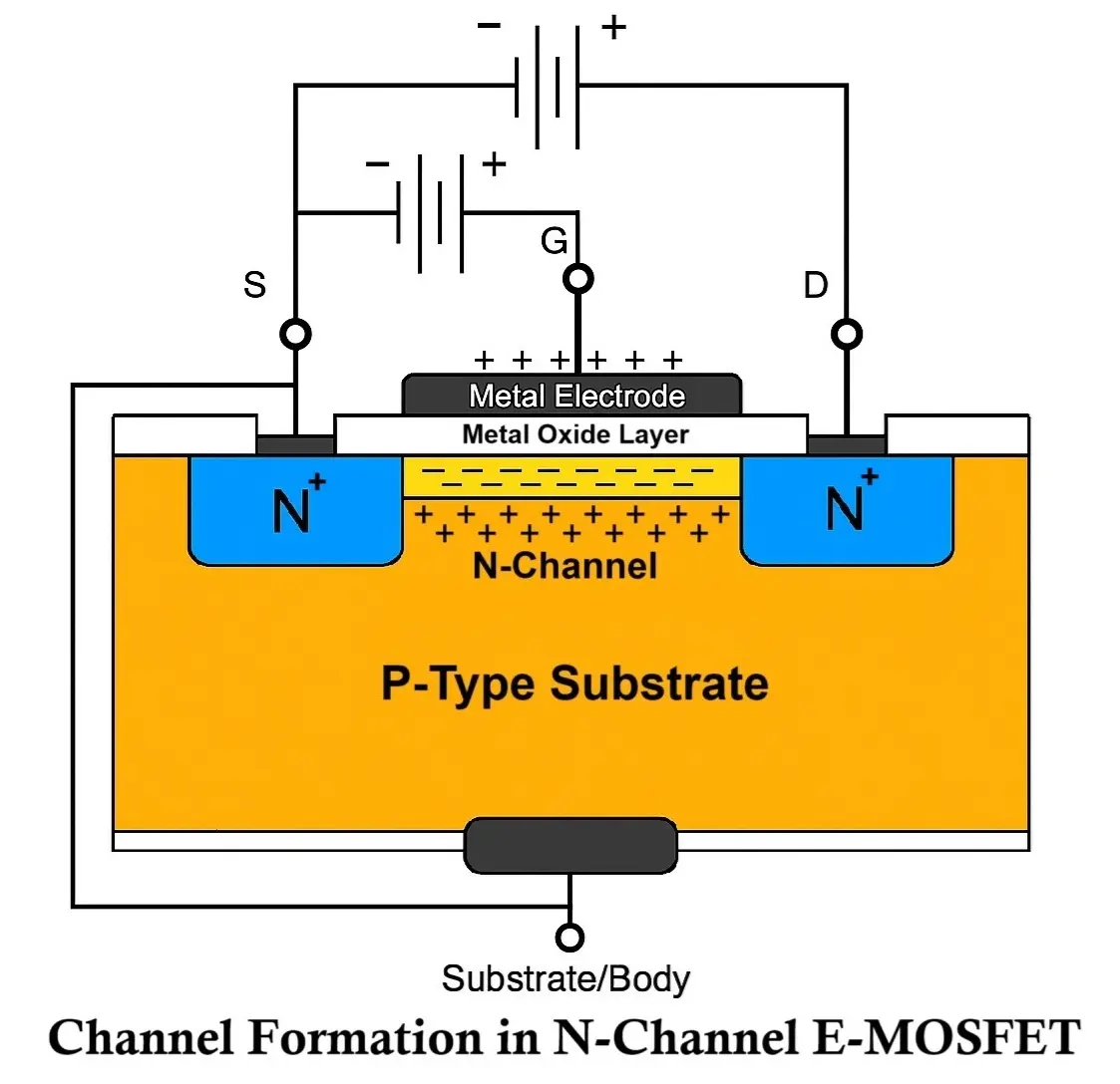
The construction of a MOSFET is rooted in precise semiconductor fabrication processes such as doping, oxidation, and thin-film deposition. To understand the internal structure clearly, let us consider an N-channel MOSFET, which is the most widely used type in practical applications.

Basic Semiconductor Structure
The MOSFET is fabricated on a P-type semiconductor substrate, which serves as the body (or bulk) of the device. This substrate provides the foundation upon which the active regions of the transistor are formed.
- Within this P-type substrate:
- Two heavily doped N-type (N⁺) regions are created
- These regions form the Source (S) and Drain (D) terminals
- The region between them is initially non-conductive, as it lacks free electrons
This gap between source and drain is known as the channel region, and its conductivity is controlled externally by the gate terminal.
Gate Oxide Layer (SiO₂)
A very thin insulating layer of silicon dioxide (SiO₂) is grown over the channel region using thermal oxidation. This oxide layer is one of the most critical parts of the MOSFET structure.
- Its key roles include:
- Electrical insulation between the gate and the substrate
- Prevention of direct current flow into the gate
- Allowing the gate to control the channel using an electric field
The thickness of this oxide layer is extremely small (typically in the nanometer range in modern devices), which enhances capacitive coupling while maintaining insulation.
Gate Terminal Formation
On top of the SiO₂ layer, a conductive material is deposited to form the Gate (G) terminal. This material can be:
- Metal (in early MOSFETs)
- Polysilicon (commonly used in modern fabrication)
The gate, oxide, and substrate together form a structure similar to a parallel-plate capacitor, commonly referred to as a MOS capacitor.
MOS Capacitor Concept
The MOSFET structure inherently behaves like a capacitor:
- Gate → one plate
- Substrate → second plate
- SiO₂ layer → dielectric medium
When a voltage is applied to the gate, an electric field is established across the oxide layer. This field penetrates into the substrate and influences the charge distribution in the channel region.
This capacitive effect is the fundamental mechanism that enables the MOSFET to control current flow without direct electrical conduction through the gate.
Channel Formation and Field Control
A crucial aspect of MOSFET construction is that:
- There is no physical conductive path between gate and channel
- The gate influences the channel purely through an electric field
When a suitable voltage is applied to the gate:
- Charge carriers (electrons in N-channel MOSFET) are attracted toward the oxide-substrate interface
- A conductive inversion layer (channel) is formed between source and drain
- This allows current to flow when a voltage is applied across drain and source
This mechanism is why the MOSFET is classified as a Field-Effect Transistor (FET) – its operation depends on the electric field rather than current injection.
Structural Insights
- Source and drain are symmetrical in structure, but differ in biasing during operation
- The body is often internally connected to the source in discrete devices
- The quality and thickness of the oxide layer directly affect device performance, leakage, and reliability
- Modern MOSFETs use advanced fabrication techniques (e.g., high-k dielectrics, FinFET structures) to improve efficiency and scaling
This carefully engineered structure enables MOSFETs to achieve high input impedance, low power consumption, and excellent switching performance, making them indispensable in modern electronics.
Working Principle of MOSFET
The working principle of a MOSFET is fundamentally based on electric field control of charge carriers. To develop a clear and practical understanding, we analyze the operation of an N-channel enhancement MOSFET, which is the most widely used configuration in both analog and digital circuits.
Initial Condition: Cut-off Region (VGS = 0)
When no voltage is applied between the gate and source:
- No electric field exists across the oxide layer
- The region between source and drain remains non-conductive
- (VGS = 0)
Since the substrate is P-type and there are no free electrons forming a channel:
- No current flows between drain and source
- The MOSFET behaves like an open switch
This state is called the cut-off region.
Application of Gate Voltage and Channel Formation
When a positive voltage is applied to the gate:
- An electric field develops across the SiO₂ layer
- This field repels holes (majority carriers in P-substrate)
- Simultaneously, it attracts electrons toward the oxide-substrate interface
As the gate voltage increases:
- Electron concentration at the surface increases
- A thin conductive layer begins to form
- This layer is known as the inversion layer or channel
Threshold Voltage (Vth)
The formation of a stable conductive channel occurs only when the gate voltage exceeds a critical value called the threshold voltage VTH.
- If ( VGS < VTH ): No conduction (device OFF)
- If ( VGS >= VTH ): Channel forms and conduction begins
Thus, VTH represents the minimum gate voltage required to “turn ON” the MOSFET.
Drain Current Flow (Applying VDS)
Once the channel is formed and a voltage is applied between drain and source:
- ( VDS > 0 )
- Electrons flow from source → drain (actual electron flow)
- Conventional current flows from drain → source
- The magnitude of drain current ID depends on:
- Gate-to-source voltage VGS
- Drain-to-source voltage VDS
Modes of Operation
As VDS increases, the MOSFET transitions through distinct operating regions:
Linear Region (Ohmic Region)
- Condition: VGS > VTH and VDS is small
- Behavior:
- Channel is fully formed along entire length
- MOSFET behaves like a voltage-controlled resistor
- Current increases approximately linearly with ( VDS )
- Key Insight: Resistance of the channel is controlled by ( VGS )
Saturation Region (Active Region)
- Condition: VDS >= VGS – VTH
- Behavior:
- Channel near the drain narrows and eventually pinches off
- Current no longer increases significantly with ( VDS )
- Drain current becomes primarily dependent on ( VGS )
- This is the region used in:
- Amplifiers
- Analog signal processing
Pinch-Off Phenomenon
As VDS increases further:
- The channel near the drain collapses (pinch-off point)
- However, current continues due to carrier drift in the electric field
- This leads to a constant current behavior
Mathematical Insight
In saturation, the drain current is approximately proportional to the square of the effective gate voltage:
ID ∝ (VGS - VTH)²
This quadratic relationship is fundamental to analog MOSFET operation and gain control.
Key Functional Understanding
- MOSFET is a voltage-controlled current device
- Gate voltage controls:
- Channel formation
- Channel conductivity
- Drain current magnitude
- Unlike BJTs:
- No input current is required to control output
- Control is achieved purely via electric field modulation
Practical Interpretation
- Digital circuits:
MOSFET operates as a switch (cut-off ↔ saturation) - Analog circuits:
Operates in saturation for amplification - Power electronics:
Often used in linear and switching regions for efficiency control
This electric-field-based control mechanism is what makes MOSFETs extremely efficient, scalable, and suitable for modern high-speed electronic systems.
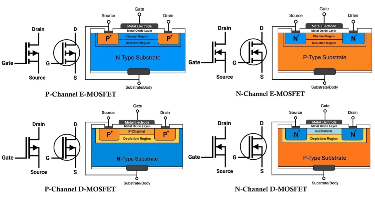
Types and Classifications of MOSFET
MOSFETs are broadly classified based on two fundamental criteria: mode of operation and type of charge carrier. This classification is essential because it directly determines how the device behaves in a circuit, its switching characteristics, and its suitability for specific applications.
Based on Mode of Operation
This classification depends on whether the MOSFET requires an external voltage to conduct or not.
Enhancement-Mode MOSFET (E-MOSFET)
Enhancement-mode MOSFETs are the most widely used type in modern electronics.

- Key Characteristics:
- Device is normally OFF when ( VGS = 0 )
- No channel exists initially between source and drain
- A gate voltage must be applied to induce (enhance) the channel
- Conduction starts only when ( VGS > VTH )
- Operational Insight:
- For N-channel: positive gate voltage is required
- For P-channel: negative gate voltage is required
- Applications:
- Digital logic circuits (switching operation)
- Power electronics (SMPS, motor drivers)
- Microprocessors and ICs
Because of their low standby power consumption and excellent switching performance, enhancement MOSFETs dominate practical circuit design.
Depletion-Mode MOSFET (D-MOSFET)
Depletion-mode MOSFETs behave quite differently.

- Key Characteristics:
- Device is normally ON when (VGS = 0)
- A channel already exists without gate bias
- Applying gate voltage reduces (depletes) the channel conductivity
- Operational Insight:
- For N-channel: negative gate voltage reduces current
- Positive voltage can further enhance conduction
- Applications:
- Analog circuits
- Constant current sources
- Special-purpose amplifiers
Although less common than enhancement MOSFETs, depletion devices are useful where default conduction is required.
Based on Channel Type
This classification depends on the type of charge carriers responsible for conduction.
N-Channel MOSFET (NMOS)
In NMOS devices electrons act as majority carriers and conductivity is due to negative charge carriers
- Advantages:
- Higher carrier mobility → faster switching speed
- Lower ON resistance → higher efficiency
- Better current handling capability
- NMOS transistors are preferred in:
- High-speed switching circuits
- Power electronics
- Digital IC design (as pull-down networks)
P-Channel MOSFET (PMOS)
In PMOS devices holes act as majority carriers and conductivity is based on positive charge carriers
- Characteristics:
- Lower mobility compared to electrons
- Slower switching speed
- Higher ON resistance than NMOS
- Applications:
- Used in complementary configurations
- High-side switching (simpler gate drive in some cases)
CMOS Technology (Complementary MOS)
One of the most important practical implementations of MOSFET technology is CMOS (Complementary MOS), which combines both NMOS and PMOS transistors in a single circuit.

- Basic Concept
- NMOS and PMOS are arranged in a complementary manner
- When one transistor is ON, the other is OFF
- This eliminates direct current paths between supply and ground in steady state
- Key Advantages
- Extremely low static power consumption
- High noise immunity
- High packing density (billions of transistors per chip)
- Excellent scalability for VLSI design
- Typical Applications
- Microprocessors
- Memory devices (RAM, ROM)
- Digital logic circuits (inverters, gates, flip-flops)
- Functionality
- In a CMOS inverter:
- PMOS pulls output HIGH
- NMOS pulls output LOW
- Only one conducts at a time → minimal power loss
Classification Summary
| Classification | Type | Default State | Key Feature |
|---|---|---|---|
| Mode | Enhancement | OFF | Requires gate voltage |
| Mode | Depletion | ON | Gate voltage reduces conduction |
| Channel | NMOS | — | Fast, efficient (electron conduction) |
| Channel | PMOS | — | Complementary operation (hole conduction) |
This classification framework is crucial for selecting the right MOSFET in circuit design, whether the goal is high-speed switching, low power consumption, or analog signal control.
MOSFET Characteristics
The electrical behavior of a MOSFET—whether enhancement or depletion type, N-channel or P-channel—is primarily described using two fundamental characteristic curves:
- Output Characteristics → ID vs VDS
- Transfer Characteristics → ID vs VGS
These curves are essential for understanding device operation, biasing, and performance in both analog and switching applications.
Output Characteristics (ID vs VDS)
This set of curves shows how the drain current ID varies with drain-source voltage VDS for different values of gate-source voltage VGS.

Behavior in Different Regions
(a) Cut-off Region
- Condition: VGS < VTH (Enhancement NMOS)
- Channel is not formed ID ≈ 0
For depletion MOSFET, this region occurs when gate voltage is sufficiently negative (NMOS) or positive (PMOS) to suppress conduction.
(b) Linear (Ohmic) Region
- Condition: VDS is small and VGS > VTH
- Characteristics:
- Current increases linearly with ( VDS )
- MOSFET behaves like a voltage-controlled resistor
- Channel is uniform along its length
- Applicable to:
- Both enhancement and depletion types
- Used in analog variable resistance applications
(c) Saturation Region
- Condition: VDS >= VGS – VTH
- Characteristics:
- Channel becomes pinched off near the drain
- Drain current becomes nearly constant
- ID mainly depends on VGS, not VDS
- Used in: Amplifier circuits and constant current sources

Important Note (N vs P Channel)
- NMOS: Positive VGS, current flows with electrons
- PMOS: Negative VGS, curves are mirror image (inverted polarity)
- Voltage handling VDS(max) is not fundamentally limited by channel type. Both N-channel and P-channel MOSFETs can be designed for high voltages.
- However, in real devices, P-channel MOSFETs usually have lower voltage ratings and worse performance than comparable N-channel parts.
Transfer Characteristics (ID vs VGS)
This curve describes how the drain current varies with gate voltage, typically in the saturation region.

For Enhancement MOSFET
- When VGS < VTH: ID ≈ 0
- When VGS > VTH: Channel forms and ID increases rapidly (quadratically)
ID ∝ (VGS - VTH)²

For Depletion MOSFET
- At VGS = 0: Device is already conducting
- Applying opposite polarity gate voltage:
- Reduces channel conductivity
- Eventually turns device OFF
- Applying same polarity enhances current further
Comparative Insight (All Types)
| Type | Default State | Control Mechanism |
|---|---|---|
| Enhancement NMOS | OFF | Positive ( VGS ) creates channel |
| Enhancement PMOS | OFF | Negative ( VGS ) creates channel |
| Depletion NMOS | ON | Negative ( VGS ) reduces current |
| Depletion PMOS | ON | Positive ( VGS ) reduces current |
Key MOSFET Parameters
Understanding these parameters is critical for design, modeling, and practical application.
Threshold Voltage ( VTH)
- Minimum gate voltage required to initiate conduction
- Typical range: 1V to 4V (varies by device)
- Determines switching point in digital circuits
VDS(sat) (Drain-Source Saturation Voltage)
- Minimum drain-source voltage required to enter saturation region
- Occurs when: VDS = (VGS − VTH)
- Beyond this point, drain current becomes nearly constant
- Separates triode (linear) and saturation regions
- Critical for MOSFET amplifier and switching operation
Pinch-Off Voltage (VP)
- Gate-source voltage at which the channel is completely cut off
- Drain current becomes nearly zero
- For n-channel devices, VP is negative
- Also called cutoff voltage (VGS(off))
- Important in JFET and depletion-type MOSFET operation
IDSS (Drain-Source Saturation Current)
- Maximum drain current when VGS = 0 (for depletion-type MOSFET/JFET)
- Represents device’s natural conduction level without gate bias
- Occurs in saturation region
- Used as a key parameter in transfer characteristics
- Device-specific constant (given in datasheet)
Transconductance (gm)
- Indicates gain capability of the MOSFET
- Defined as: gm = dID / dVGS
- Higher gm → better amplification performance
Drain Resistance (RDS(on))
- Resistance between drain and source in ON state
- Lower RDS(on) → higher efficiency
- Critical in: Power electronics and switching regulators
Breakdown Voltage
- Maximum VDS the MOSFET can withstand before failure
- Exceeding this leads to avalanche breakdown
- Important for high-voltage applications
The characteristic curve shows the behavior of all MOSFET types:
- Enhancement vs Depletion → determines default conduction
- NMOS vs PMOS → determines carrier type and polarity
- Regions of operation → determine functional role in circuits
- Digital Electronics: Operate between cut-off and saturation → switching behavior
- Analog Circuits: Use saturation region → controlled current source
- Power Applications: Use linear + saturation regions depending on switching mode
Advantages and Disadvantages of MOSFET
MOSFETs have become the dominant semiconductor device in modern electronics due to their exceptional electrical characteristics and scalability. However, like any device, they come with inherent limitations that must be considered during design and application.
Advantages of MOSFET
Extremely High Input Impedance
One of the most significant advantages of MOSFETs is their very high input impedance, typically ranging from megaohms to gigaohms.
- Reason:
- The gate is insulated from the channel by a SiO₂ layer
- Practically no gate current flows
- Impact:
- Minimal loading on previous circuit stages
- Ideal for signal processing and sensor interfacing
- Improved overall circuit efficiency
Voltage-Controlled Operation
MOSFETs are voltage-controlled devices, unlike BJTs which are current-controlled.
- Implications:
- Simplified driving circuitry
- Lower input power requirements
- Easier integration into digital logic systems
This makes MOSFETs highly suitable for logic gates, microcontrollers, and embedded systems.
High-Speed Switching Capability
MOSFETs can switch extremely fast, often in nanoseconds.
- Reason:
- No minority carrier storage (unlike BJTs)
- Operation based on majority carriers only
- Applications:
- Switch Mode Power Supplies (SMPS)
- DC-DC converters
- High-frequency amplifiers
- Digital circuits and processors
Low Power Consumption (Especially CMOS)
- In CMOS (Complementary MOS) configurations:
- Power is consumed mainly during switching
- Negligible static power dissipation
- Useful in highly energy-efficient systems
- Essential for:
- Battery-operated devices
- Mobile electronics
- Large-scale integrated circuits
- Essential for:
Scalability and Integration Capability
MOSFETs can be fabricated at extremely small sizes using modern semiconductor processes.
- Integration of billions of transistors on a single IC enables:
- Microprocessors
- Memory chips
- System-on-Chip (SoC) designs
This scalability is the foundation of modern computing and VLSI technology.
Low ON Resistance RDS(on)
- In power MOSFETs drain-to-source resistance is very low when ON
- This results in reduced conduction losses and higher efficiency
- This is Critical in power electronics, motor drivers, inverters and SMPS
Thermal Stability
MOSFETs exhibit positive temperature coefficient of resistance:
- As temperature increases → resistance increases
- This helps prevent thermal runaway
- Advantage over BJTs:
- Easier parallel operation
- Improved reliability in power systems
Disadvantages of MOSFET
Sensitivity to Electrostatic Discharge (ESD)
The thin gate oxide layer (SiO₂) is extremely delicate.
- Problem:
- High static voltage can puncture the oxide layer
- Leads to permanent device failure
- Precautions:
- Use anti-static handling techniques
- Proper grounding and ESD protection circuits
Gate Oxide Breakdown
Apart from ESD, excessive gate voltage can also damage the device.
- Condition: ( VGS ) exceeding rated limits
- Effect: Irreversible breakdown of insulation and loss of control over channel
Designers must ensure proper gate drive voltage control.
High Initial Cost (in Some Applications)
While MOSFETs are cheap in mass production:
- High-performance or power MOSFETs can be costly
- Advanced fabrication technology increases design complexity
Thermal Management in Power Applications
- In high-power circuits significant power dissipation occurs and heat generation can degrade performance
- Requirements: Heat sinks, cooling systems, thermal design considerations
- Failure to manage heat leads to reduced efficiency and device failure
Limited Voltage Handling (Compared to Some Devices)
- Although power MOSFETs handle high voltages, they may be less suitable than IGBTs for very high voltage applications.
- There is a Trade-off between switching speed and voltage rating
Susceptibility to Noise and Parasitics
- MOSFETs are sensitive to:
- Parasitic capacitances (gate-drain, gate-source)
- High-frequency noise
- Effects: Unwanted oscillations, switching losses and EMI issues
- Careful PCB layout and gate drive design are required.
Complex Fabrication Process
- MOSFET manufacturing involves:
- Advanced lithography
- Precise oxide growth
- Controlled doping
- This increases fabrication complexity and cost of semiconductor facilities
Advantages and Disadvantages Summary
| Advantage | Engineering Benefit |
|---|---|
| High input impedance | Minimal loading |
| Fast switching | High-frequency operation |
| Low power consumption | Efficient systems |
| Scalability | VLSI and IC fabrication |
| Limitation | Design Challenge |
|---|---|
| ESD sensitivity | Requires protection |
| Thermal issues | Needs heat management |
| Gate breakdown | Careful biasing required |
| Parasitics | Advanced design needed |
MOSFETs represent a near-ideal switching and amplification device in modern electronics. Their advantages overwhelmingly outweigh their limitations, which is why they dominate:
- Digital electronics (CMOS logic)
- Power electronics (SMPS, converters)
- Analog circuits (amplifiers, signal processing)
However, achieving optimal performance requires careful attention to thermal design, voltage limits, and protection mechanisms.
This is why MOSFETs remain the cornerstone of modern electronics, from nanoscale ICs to high-power industrial systems.
Applications of MOSFET
MOSFETs are among the most widely used semiconductor devices due to their high efficiency, fast switching speed, and scalability. Their applications span across digital, analog, and power electronics, making them indispensable in modern engineering systems.
Digital Electronics and Computing Systems
MOSFETs form the backbone of modern digital electronics, enabling the operation of virtually all computing devices.
- They are widely used in:
- Logic gates (AND, OR, NOT, NAND, NOR)
- Microprocessors and microcontrollers
- Memory devices (RAM, ROM, Flash)
A key implementation is CMOS technology, where NMOS and PMOS transistors are used in a complementary configuration. This provides:
- Ultra-low static power consumption
- High noise immunity
- Extremely high integration density
As a result, billions of MOSFETs can be integrated into a single chip, forming the foundation of computers, smartphones, and embedded systems.
Power Electronics
MOSFETs play a crucial role in high-efficiency power conversion systems, where switching performance is critical.
- Common applications include:
- Switch Mode Power Supplies (SMPS)
- DC-DC converters (buck, boost, buck-boost)
- Inverters (DC to AC conversion)
- Voltage regulators
- Their effectiveness comes from key properties:
- High switching speed, reducing switching losses
- Low RDS(on), minimizing conduction losses
- High efficiency at elevated frequencies
These characteristics enable compact designs, improved energy efficiency, and reduced heat generation.
Amplifiers (Analog and RF)
In analog electronics, MOSFETs are widely used for signal amplification due to their favorable electrical characteristics.
- Typical applications include:
- Audio amplifiers
- RF amplifiers
- Low-noise amplifiers (LNA)
- They offer several advantages:
- High input impedance, minimizing signal loading
- Low noise performance
- Good linearity in the saturation region
For amplification, MOSFETs are typically operated in the saturation region, making them suitable for both small-signal and high-frequency applications.
Motor Control Systems
MOSFETs are essential components in motor control circuits, particularly where efficiency and precision are required.
- They are commonly used in:
- H-Bridge circuits for bidirectional control
- PWM-based speed control systems
- Brushless DC (BLDC) motor drivers
- Their advantages include:
- Fast switching for precise control
- High efficiency with reduced power loss
- Capability to handle high currents
These features make them ideal for robotics, electric vehicles (EVs), and industrial automation systems.
LED Drivers and Lighting Systems
MOSFETs are widely used in modern lighting systems, especially for efficient LED operation.
- They perform functions such as:
- Current regulation
- PWM-based dimming control
- Switching in LED power supplies
- This results in:
- High efficiency
- Extended LED lifespan
- Accurate brightness control
Battery Management Systems (BMS)
MOSFETs are critical in battery protection and control circuits, ensuring safe and efficient operation.
- They are used for:
- Overcharge protection
- Over-discharge protection
- Current limiting
- Cell balancing
Their advantages in BMS applications include fast switching response, low conduction losses, and reliable performance.
Renewable Energy Systems
In renewable energy systems, MOSFETs are used to improve energy conversion and efficiency.
- Key applications include:
- Solar inverters
- Wind energy converters
- Energy storage systems
- They support functions such as:
- DC-AC conversion
- Power optimization
- Maximum Power Point Tracking (MPPT)
This leads to improved efficiency, reduced energy loss, and more compact system designs.
High-Frequency and Switching Applications
Due to their majority carrier operation, MOSFETs are highly suitable for high-frequency applications.
- They are used in:
- RF switching circuits
- High-frequency oscillators
- Communication systems
MOSFETs are a universal semiconductor device used across multiple domains:
- Digital systems → computation and logic
- Power systems → energy conversion and control
- Analog systems → amplification and signal processing
Their unique combination of speed, efficiency, and scalability makes them the fundamental building block of nearly every modern electronic system.
Comparison with BJT, IGBT and JFET
To fully appreciate the importance of MOSFETs, it is essential to compare them with other commonly used transistor devices such as Bipolar Junction Transistor (BJT) and Junction Field Effect Transistor (JFET). Each device has its own operational principles, advantages, and limitations.
MOSFET vs BJT
In a BJT, a continuous base current is required to control the collector current, whereas in a MOSFET, the gate draws negligible current, requiring only a voltage to operate.
- MOSFET: Voltage-controlled device
- BJT: Current-controlled device
Comparison
| Parameter | MOSFET | BJT |
|---|---|---|
| Control Mechanism | Voltage-controlled | Current-controlled |
| Input Impedance | Very high | Low |
| Switching Speed | Very fast | Slower (due to charge storage) |
| Power Consumption | Low | Higher |
| Carrier Type | Majority carriers | Minority + majority carriers |
| Thermal Stability | Better (no thermal runaway) | Prone to thermal runaway |
- MOSFETs eliminate base current losses, improving efficiency
- BJTs suffer from minority carrier storage, which slows switching
- MOSFETs are preferred in:
- High-frequency circuits
- Digital systems
- Power switching applications
However, BJTs may still be used where high gain and linearity are required in certain analog designs.
MOSFET vs IGBT
Both devices are controlled by gate voltage, but an IGBT combines the high input impedance of a MOSFET with the current conduction capability of a BJT.
- MOSFET: Voltage-controlled device
- IGBT: Voltage-controlled device with bipolar conduction
In a MOSFET, conduction occurs through majority carriers only, whereas in an IGBT, conduction involves both majority and minority carriers, leading to different switching and conduction characteristics.
Comparison
| Parameter | MOSFET | IGBT |
|---|---|---|
| Control Mechanism | Voltage-controlled | Voltage-controlled |
| Input Impedance | Very high | Very high |
| Switching Speed | Very fast | Slower (due to minority carriers) |
| Power Loss | Low at low voltage | Lower at high voltage |
| Carrier Type | Majority carriers | Minority + majority carriers |
| Voltage Rating | Low to medium | High |
| Thermal Behavior | Stable | Good but needs thermal management |
- MOSFETs switch faster because they do not involve minority carriers
- IGBTs handle higher voltages and currents more efficiently
- MOSFETs are preferred in:
- High-frequency switching circuits
- Low to medium power applications
- SMPS and DC-DC converters
- IGBTs are preferred in:
- High-voltage applications
- Motor drives
- Inverters and industrial power systems
However, IGBTs may introduce switching losses at high frequencies, making MOSFETs more suitable for fast-switching applications, while IGBTs dominate in high-power, high-voltage environments.
MOSFET vs JFET
This insulation gives MOSFETs a significant advantage in terms of input characteristics.
- MOSFET: Insulated gate (SiO₂ layer)
- JFET: Gate forms a PN junction with the channel
Comparison
| Parameter | MOSFET | JFET |
|---|---|---|
| Gate Structure | Insulated (oxide layer) | PN junction |
| Input Impedance | Extremely high | High (but lower than MOSFET) |
| Operating Modes | Enhancement + Depletion | Only Depletion |
| Gate Current | Negligible | Small leakage current |
| Control | Electric field (capacitive) | Reverse-biased junction |
- MOSFETs offer greater flexibility due to dual-mode operation
- JFETs are inherently normally ON devices
- MOSFETs dominate modern electronics due to:
- Better scalability
- Compatibility with IC fabrication
- Higher integration capability
JFETs are still used in:
- Low-noise analog front-end circuits
- High-input-impedance amplifiers
Conclusion
The MOSFET stands as a cornerstone of modern electronics, enabling the development of compact, efficient, and high-performance systems. Its defining characteristics such as high input impedance, fast switching speed, and low power consumption makes it indispensable across both analog and digital domains.
From advanced microprocessors containing billions of transistors to high-power switching systems used in industrial and renewable energy applications, MOSFETs play a critical role in shaping contemporary technology.
Compared to devices like BJTs, IGBTs and JFETs, MOSFETs offer superior scalability, efficiency, and integration capability, which is why they dominate modern circuit design, particularly in CMOS technology.
For engineering students and practitioners, a thorough understanding of MOSFET construction, operation, characteristics, and practical behavior forms the foundation for advanced topics such as:
- VLSI (Very Large-Scale Integration) design
- Power electronics (SMPS, converters, inverters)
- Embedded systems and digital architecture
Mastering MOSFETs is therefore not just important, it is essential for anyone working in modern electronics and electrical engineering.
Popular Enhancement Type MOSFETs: BS107, BS108, 2N7000, IRFZ44N.
Popular Depletion Type MOSFETs: IXTP01N100D, CPC3710, DN2540, LND150.
JFET Junction Field Effect Transistors Working and Applications
IGBT Full Form, Symbol, Construction, Working and Applications
