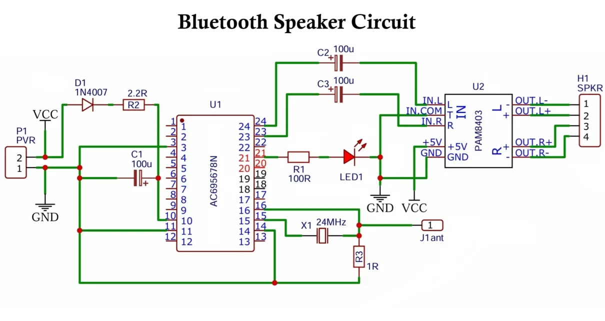
Here is a compact stereo Bluetooth speaker circuit design based on AC695678N Bluetooth audio SoC and the PAM8403 Class-D stereo audio amplifier. The circuit receives audio wirelessly from a smartphone or laptop, processes the audio inside the Bluetooth IC, amplifies the audio signal using the PAM8403 amplifier, and finally drives stereo speakers.
The circuit is simple, inexpensive, compact, and highly efficient, making it an excellent educational project for understanding modern wireless audio electronics.
Bluetooth speakers have become one of the most widely used wireless audio devices due to their portability, compact size, and ease of connectivity. Internally, a Bluetooth speaker combines three major functions into a single system:
- Wireless Bluetooth audio reception
- Digital-to-analog audio processing
- Audio power amplification for speakers
Overview of the Bluetooth Speaker Circuit
The complete circuit can be divided into the following functional sections:
- Power Supply and Protection Section
- Bluetooth Audio Receiver Section
- Crystal Oscillator and RF Section
- Audio Signal Coupling Section
- Audio Power Amplifier Section
- Speaker Output Section
- LED Status Indication Section
Each block performs a specific function, and together they create a fully functional stereo Bluetooth speaker system.

- Related Articles:
- TDA2030 Audio Amplifier Circuit: Mono, Stereo and Bass Amplifier
- LA3600 5 Band Audio Equalizer Circuit – Bass Mid Treble Control
- 12V 5A SMPS: Switched Mode Power Supply Circuit IC TOP227YN
- Digital to Analog Converter (DAC) Block Diagram, Working & Types
- Analog to Digital Converter ADC – Block Diagram & Working
- Difference Between Amplifier and Oscillator
Main Components Used in the Circuit
| Component | Value / Part Number | Description |
|---|---|---|
| U1 | AC695678N | Bluetooth audio receiver IC |
| U2 | PAM8403 | Stereo Class-D audio amplifier |
| D1 | 1N4007 | Reverse polarity protection diode |
| R1 | 100Ω | LED current limiting resistor |
| R2 | 2.2Ω | Input surge current limiting resistor |
| R3 | 1Ω | RF matching resistor |
| C1 | 100µF | Power supply filter capacitor |
| C2 | 100µF | Left channel coupling capacitor |
| C3 | 100µF | Right channel coupling capacitor |
| X1 | 24MHz Crystal | Clock oscillator for Bluetooth IC |
| LED1 | Red LED | Status indicator |
| P1 | Power Connector | 5V input supply connector |
| H1 | Speaker Connector | Stereo speaker output connector |
| J1 | Antenna Terminal | Bluetooth antenna connection |
Complete Circuit Operation
The working of the circuit begins when a 5V DC supply is applied at the input connector. The supply first passes through the protection stage, after which the Bluetooth IC initializes itself using the 24MHz crystal oscillator.
Once powered, the Bluetooth IC starts searching for nearby Bluetooth devices. When a smartphone or laptop pairs with the circuit, digital audio data is received wirelessly through the antenna.
The Bluetooth IC internally decodes the digital audio stream and generates left and right analog audio signals. These low-level audio signals are coupled through electrolytic capacitors into the PAM8403 amplifier IC.
The PAM8403 amplifies the audio signals with high efficiency and delivers sufficient power to drive stereo speakers connected at the output.
Meanwhile, the LED indicator displays the operating or pairing status of the Bluetooth module.
Power Supply and Protection Section
The power supply section provides stable DC voltage to the Bluetooth receiver IC and the audio amplifier.
This section consists of:
- P1 input connector
- D1 reverse polarity protection diode
- R2 surge current limiting resistor
- C1 filter capacitor
Power Input Connector (P1)
P1 is the main DC power input terminal.
| Pin | Connection |
|---|---|
| Pin 1 | Ground (GND) |
| Pin 2 | Positive VCC input |
The circuit is designed to operate from a regulated 5V DC supply.
Possible power sources include:
- USB power supply
- Mobile charger
- Lithium battery with boost converter
- Power bank
- 5V adapter
Reverse Polarity Protection Diode (D1)
1N4007 Rectifier Diode D1 protects the circuit against accidental reverse connection of the power supply.
If the battery or adapter polarity is accidentally reversed:
- The diode blocks current flow.
- The sensitive ICs remain protected.
- Circuit damage is prevented.
Without this diode, the Bluetooth IC and amplifier could be permanently damaged.
| Diode Terminal | Connected To |
|---|---|
| Anode | Positive supply input |
| Cathode | R2 resistor |
Current path: VCC → D1 → R2 → Main Supply Rail
Current Limiting Resistor (R2)
2.2Ω resistor R2 limits sudden inrush current when the circuit is powered ON.
It also helps in:
- Reducing switching noise
- Protecting the IC during surges
- Suppressing transient spikes
- Improving supply stability
Although the resistance value is small, it plays an important role in improving overall circuit reliability.
| Terminal | Connected To |
|---|---|
| One side | Cathode of D1 |
| Other side | Main VCC supply rail |
Power Filter Capacitor (C1)
100µF electrolytic capacitor C1 filters unwanted ripple and voltage fluctuations from the power supply. Bluetooth and audio circuits are sensitive to noise.
Without proper filtering:
- Audio distortion may occur
- Bluetooth signal instability may appear
- Amplifier noise may increase
- Random resets may happen
The capacitor acts like a temporary energy storage device and stabilizes the supply voltage during sudden load variations.
| Capacitor Terminal | Connected To |
|---|---|
| Positive terminal | VCC rail |
| Negative terminal | Ground |
The capacitor is connected across the power supply rails.

Bluetooth Audio Receiver Section
The Bluetooth receiver section is the heart of the entire circuit. This section uses U1 AC695678N Bluetooth Audio IC
AC695678N Bluetooth Audio IC: The AC695678N is an integrated Bluetooth audio SoC (System on Chip). It combines several functions internally.
- Bluetooth transceiver
- Audio decoder
- Microcontroller unit
- Audio DAC
- RF synthesizer
- Digital signal processing
- Stereo audio output circuitry
Because multiple blocks are integrated into a single chip, the external component count is greatly reduced.
Main Functions of the Bluetooth IC
- Bluetooth Communication: The IC receives wireless audio data from paired devices.
- Digital Audio Decoding: Compressed Bluetooth audio data is decoded internally.
- Audio Signal Generation: The IC generates analog left and right audio signals.
- System Control: The IC controls Pairing, LED indication, Audio synchronization and Wireless communication.
Power Connections of U1
Several pins of the IC are connected to Ground. This is common in RF and audio ICs because separate internal blocks require stable supply paths. Multiple ground pins help reduce RF interference, audio noise and signal instability.
Crystal Oscillator and RF Section
Bluetooth communication requires an accurate and stable clock signal.
This section consists of:
- 24MHz crystal oscillator
- RF antenna network
- Matching resistor
24MHz Crystal Oscillator (X1)
The crystal generates a precise clock frequency required by the Bluetooth IC.
The oscillator signal is essential for:
- RF carrier generation
- Timing synchronization
- Audio data processing
- Internal processor operation
Without a stable clock source, Bluetooth communication becomes unreliable.
| Crystal Terminal | Connected To |
|---|---|
| One terminal | Pin 15 |
| Other terminal | Pin 16 / antenna side |
The crystal should be placed physically close to the IC on the PCB to minimize noise and improve frequency stability.
RF Matching Resistor (R3)
1Ω resistor R3 forms part of the antenna matching network.
The resistor helps in:
- RF impedance stabilization
- Reducing signal reflection
- Improving antenna efficiency
- Noise suppression
| Terminal | Connected To |
|---|---|
| One side | RF antenna node |
| Other side | Ground |
Bluetooth Antenna Terminal (J1)
J1 is the Bluetooth RF antenna connection point.
- This antenna enables:
- Wireless signal transmission
- Bluetooth signal reception
- Device communication
- The antenna node is connected with:
- Bluetooth RF section
- Crystal network
- RF matching resistor
- Proper antenna design greatly affects:
- Wireless range
- Signal stability
- Audio streaming quality
LED Status Indicator Section
The circuit contains a status LED used for visual indication.
The LED may indicate:
- Power ON condition
- Pairing mode
- Bluetooth connection status
- Data activity
The blinking behavior depends on the firmware programmed inside the Bluetooth IC. The 100Ω resistor gives LED current limiting protection. Without a resistor, excessive current can destroy the LED. R1 safely limits the LED current.
| LED Terminal | Connected To |
|---|---|
| Anode | U1 Pin 21 via R1 |
| Cathode | Ground |
When U1 outputs a HIGH signal at pin 21, current flows through the resistor and LED, causing it to glow.
Audio Signal Coupling Section
The audio output from the Bluetooth IC cannot be directly connected to the amplifier input because unwanted DC components may be present. To solve this problem, coupling capacitors are used.
This section contains:
- C2 = Left channel coupling capacitor
- C3 = Right channel coupling capacitor
The coupling capacitors perform several important functions:
- Block DC voltage
- Pass AC audio signal
- Protect amplifier input stage
- Improve audio quality
- Prevent signal distortion
These capacitors allow only the audio waveform to pass into the amplifier.
Left Channel Coupling Capacitor (C2)
| Terminal | Connected To |
|---|---|
| Positive terminal | U1 Pin 24 |
| Negative terminal | PAM8403 Left Input |
Right Channel Coupling Capacitor (C3)
| Terminal | Connected To |
|---|---|
| Positive terminal | U1 Pin 23 |
| Negative terminal | PAM8403 Right Input |
The 100µF electrolytic capacitor transfers left and right channel audio to the amplifier stage.
PAM8403 Stereo Audio Amplifier Section
The PAM8403 is the power amplification stage of the circuit. It receives low-level audio signals from the Bluetooth IC and increases the signal power sufficiently to drive speakers.
PAM8403 Amplifier IC
- Stereo amplifier
- Class-D architecture
- High efficiency
- Low heat generation
- 5V operation
- Compact size
- Low external component count
The PAM8403 is widely used in:
- Bluetooth speakers
- Portable sound systems
- USB speakers
- DIY audio amplifiers
Why Class-D Amplifier is Used
Traditional Class-A or Class-AB amplifiers generate significant heat and waste power. The PAM8403 uses Class-D switching technology.
- High efficiency (typically above 85%)
- Low power loss
- Longer battery life
- Reduced heat generation
This makes it ideal for portable Bluetooth speaker systems.
Input Connections of PAM8403
Left Audio Input
| Pin | Connected To |
|---|---|
| IN.L | C2 output |
Right Audio Input
| Pin | Connected To |
|---|---|
| IN.R | C3 output |
Common Audio Ground
| Pin | Connected To |
|---|---|
| IN.COM | Ground |
Power Supply Connections
| Pin | Connected To |
|---|---|
| +5V | Main VCC supply |
| GND | Ground |
The amplifier shares the same 5V supply rail as the Bluetooth IC.
Speaker Output Section
The amplified stereo audio signal is delivered to the speaker connector H2. The PAM8403 provides bridge-tied load (BTL) outputs.
Left Channel Speaker Connections
| PAM8403 Pin | Function |
|---|---|
| OUT_L+ | Left speaker positive |
| OUT_L- | Left speaker negative |
Right Channel Speaker Connections
| PAM8403 Pin | Function |
|---|---|
| OUT_R+ | Right speaker positive |
| OUT_R- | Right speaker negative |
Important Note About BTL Outputs: The PAM8403 does not use ground-referenced speaker outputs.
- Speaker negative terminals must never connect to ground.
- Both speaker wires must connect directly to the amplifier outputs.
- Incorrect grounding can permanently damage the amplifier IC.
Stepwise Working of the Circuit
- Applying Power: A regulated 5V supply is applied through connector P1.
- Protection and Filtering:
- The supply passes through
- D1 for reverse polarity protection
- R2 for surge limitation
- C1 for noise filtering
- The supply passes through
- Bluetooth IC Initialization:
- The AC695678N Bluetooth IC powers ON.
- The 24MHz crystal starts oscillation and provides the required system clock.
- Bluetooth Pairing: The Bluetooth module enters pairing mode, and LED indicator may blink during this stage.
- Wireless Audio Reception: After pairing, digital audio data is received wirelessly through the antenna.
- Audio Decoding:
- The Bluetooth IC internally decodes the digital audio stream and generates
- Left channel analog audio
- Right channel analog audio
- The Bluetooth IC internally decodes the digital audio stream and generates
- Audio Coupling: C2 and C3 block unwanted DC components and pass only the AC audio signal.
- Audio Amplification: The PAM8403 amplifies both audio channels.
- Speaker Output: Amplified stereo audio is delivered to the speakers connected at h2.
Pin Connections of Bluetooth Speaker Circuit
AC695678N Bluetooth IC (U1)
| Pin Number | Connection |
|---|---|
| Pin 3, 11, 14 | Ground |
| Pin 10 | VCC |
| Pin 15, 16 | Crystal oscillator |
| Pin 21 | LED indicator circuit |
| Pin 23 | Right audio capacitor C3 |
| Pin 24 | Left audio capacitor C2 |
PAM8403 Amplifier IC (U2)
| Pin | Connection |
|---|---|
| IN.L | Left audio input |
| IN.COM | Audio ground |
| IN.R | Right audio input |
| +5V | Supply voltage |
| GND | Ground |
| OUT_L+ | Left speaker positive |
| OUT_L- | Left speaker negative |
| OUT_R+ | Right speaker positive |
| OUT_R- | Right speaker negative |
PCB Design Considerations
Bluetooth audio circuits require careful PCB design for reliable operation.
- Keep RF Traces Short: Long RF traces can reduce Bluetooth signal quality.
- Place Crystal Near IC: The 24MHz crystal should be located close to the Bluetooth IC.
- Use Proper Grounding: Poor grounding may introduce, audio hum, RF interference, Bluetooth instability.
- Separate Audio and RF Areas: RF signals may interfere with audio circuitry if layout is poor.
- Keep Antenna Area Clear: Avoid copper filling near the antenna section.
- Here is the PCB layout you can use to create your Bluetooth speaker.
Speaker Specifications
| Speaker Type | Recommended Value |
|---|---|
| Speaker impedance | 4Ω or 8Ω |
| Power rating | 3W to 5W |
| Speaker type | Full-range mini speaker |
Advantages
- Compact design
- Low component count
- Wireless audio capability
- Stereo output support
- High efficiency operation
- Low heat generation
- Low power consumption
- Portable application support
- Easy USB power compatibility
- Good sound quality for small speakers
Limitations
- Limited output power capability
- No bass control circuit
- No volume control section shown
- No battery charging system included
- RF layout sensitivity
- Basic power filtering only
Applications of the Circuit
This Bluetooth speaker circuit can be used in:
- Portable Bluetooth speakers
- Wireless stereo systems
- DIY audio projects
- Home speaker systems
- USB-powered speakers
- Battery-powered music players
- Educational electronics projects
- Compact multimedia devices
- Mini stereo sound systems
- Embedded multimedia products
Conclusion
This Bluetooth speaker circuit is a compact and efficient wireless audio system based on the AC695678N Bluetooth audio receiver IC and the PAM8403 stereo Class-D amplifier. The Bluetooth IC handles wireless communication, audio decoding, and stereo signal generation, while the PAM8403 efficiently amplifies the audio to drive stereo speakers.
The circuit also includes essential support components such as reverse polarity protection, power supply filtering, RF matching network, crystal oscillator, audio coupling capacitors, and LED status indication circuitry.
Due to its simplicity, small size, high efficiency, and low component count, this circuit is highly suitable for portable speaker applications, DIY audio systems, and educational electronics projects focused on Bluetooth audio technology.
This Bluetooth speaker circuit is a compact and efficient wireless audio solution using the AC695678N Bluetooth audio IC and PAM8403 Class-D amplifier. The Bluetooth IC receives wireless audio signals and converts them into stereo analog signals, while the PAM8403 amplifies the signals to drive stereo speakers.
The circuit includes important support sections such as reverse polarity protection, power filtering, audio coupling capacitors, crystal oscillator network, RF antenna section, and LED status indication. Due to its simplicity, low component count, and good audio performance, this circuit is highly suitable for portable Bluetooth speaker applications and electronics learning projects.
TDA2030 Audio Amplifier Circuit: Mono, Stereo and Bass Amplifier
LA3600 5 Band Graphic Audio Equalizer Circuit – Bass Mid Treble Control
12V 5A SMPS: Switched Mode Power Supply Circuit Diagram IC TOP227YN
Analog to Digital Converter (ADC) Block Diagram, Working, Types & Applications
Digital to Analog Converter (DAC) Block Diagram, Working, Types & Applications
