An extrinsic semiconductor is a semiconductor material whose electrical conductivity is intentionally increased by adding a small amount of impurity atoms into a pure semiconductor crystal. This process is known as doping. Extrinsic semiconductors form the foundation of modern electronics and are widely used in diodes, transistors, integrated circuits, LEDs, solar cells, and microprocessors.
Pure semiconductors such as silicon and germanium have limited conductivity at room temperature. By introducing controlled impurities into the crystal structure, the number of free charge carriers can be increased significantly, thereby improving conductivity and making the material suitable for practical electronic applications.
The two major types of extrinsic semiconductors are N-Type Semiconductors and P-Type Semiconductor.
- Related Articles:
- Intrinsic Semiconductors Explained
- Difference Between Intrinsic and Extrinsic Semiconductor
- Energy Band Theory of Solids: Conductors, Semiconductors, and Insulators
- Types of Diodes: Symbol, Working, Characteristics and Applications
What is an Extrinsic Semiconductor?
An extrinsic semiconductor is a semiconductor material obtained by adding impurity atoms to an intrinsic semiconductor in order to modify its electrical properties. Most common intrinsic semiconductors are Silicon (Si) and Germanium (Ge). The pentavalent or trivalent impurity atoms are called dopants, while the process of adding them is called doping.
The conductivity of a semiconductor depends on the number of free electrons and holes available for conduction. Doping increases the concentration of these charge carriers and hence increases conductivity.
Characteristics of Extrinsic Semiconductors
- Extrinsic semiconductors are semiconductors doped with impurities to increase conductivity.
- Their electrical conductivity is higher than intrinsic semiconductors.
- Doping introduces majority charge carriers.
- Two types of extrinsic semiconductors:
- n-type semiconductor → electrons are majority carriers.
- p-type semiconductor → holes are majority carriers.
- In n-type semiconductors, pentavalent impurities (donor atoms) such as phosphorus or arsenic are added.
- In p-type semiconductors, trivalent impurities (acceptor atoms) such as boron or gallium are added.
- Conductivity mainly depends on the concentration of dopants.
- They have lower resistivity compared to intrinsic semiconductors.
- Electrical conduction occurs due to both electrons and holes, but one type dominates.
- Extrinsic semiconductors are electrically neutral overall.
- They are widely used in diodes, transistors, ICs, and electronic devices.
- Their conductivity increases with temperature.
Semiconductor Doping
Doping is the process of intentionally adding a very small amount of impurity atoms to a pure semiconductor crystal to increase its conductivity. The amount of impurity added is extremely small, typically one impurity atom per millions of semiconductor atoms.
Purpose of Doping
- The main purposes of doping are:
- Increase electrical conductivity
- Control charge carrier concentration
- Create n-type and p-type materials
- Improve semiconductor device performance
- Enable fabrication of electronic components
Characteristics of Doping
- Only a very small amount of impurity is added
- The crystal structure remains almost unchanged
- Conductivity increases significantly
- The semiconductor remains electrically neutral overall
Types of Impurities
Based on the number of valence electrons, impurities are classified into two types:
| Type of Impurity | Valence Electrons | Semiconductor Formed |
|---|---|---|
| Pentavalent Impurity | 5 | N-Type Semiconductor |
| Trivalent Impurity | 3 | P-Type Semiconductor |
Pentavalent Impurity
A pentavalent impurity atom contains five valence electrons. When added to silicon or germanium, four electrons participate in covalent bonding while the fifth electron becomes free.
Such impurities are called donor impurities because they donate free electrons. Here are some examples of Pentavalent Impurities:
- Phosphorus (P)
- Arsenic (As)
- Antimony (Sb)
- Bismuth (Bi)
Trivalent Impurity
A trivalent impurity atom contains three valence electrons. When added to silicon or germanium, one covalent bond remains incomplete, creating a hole. Such impurities are called acceptor impurities because they accept electrons. Here are some examples of Trivalent Impurities:
- Boron (B)
- Gallium (Ga)
- Indium (In)
- Aluminum (Al)
Types of Extrinsic Semiconductors
Extrinsic semiconductors are classified into two types N-Type Semiconductor and P-Type Semiconductor.
Majority and Minority Carriers: In extrinsic semiconductors, one type of charge carrier dominates conduction.
| Semiconductor Type | Majority Carrier | Minority Carrier |
|---|---|---|
| N-Type | Electrons | Holes |
| P-Type | Holes | Electrons |
N-Type Semiconductor
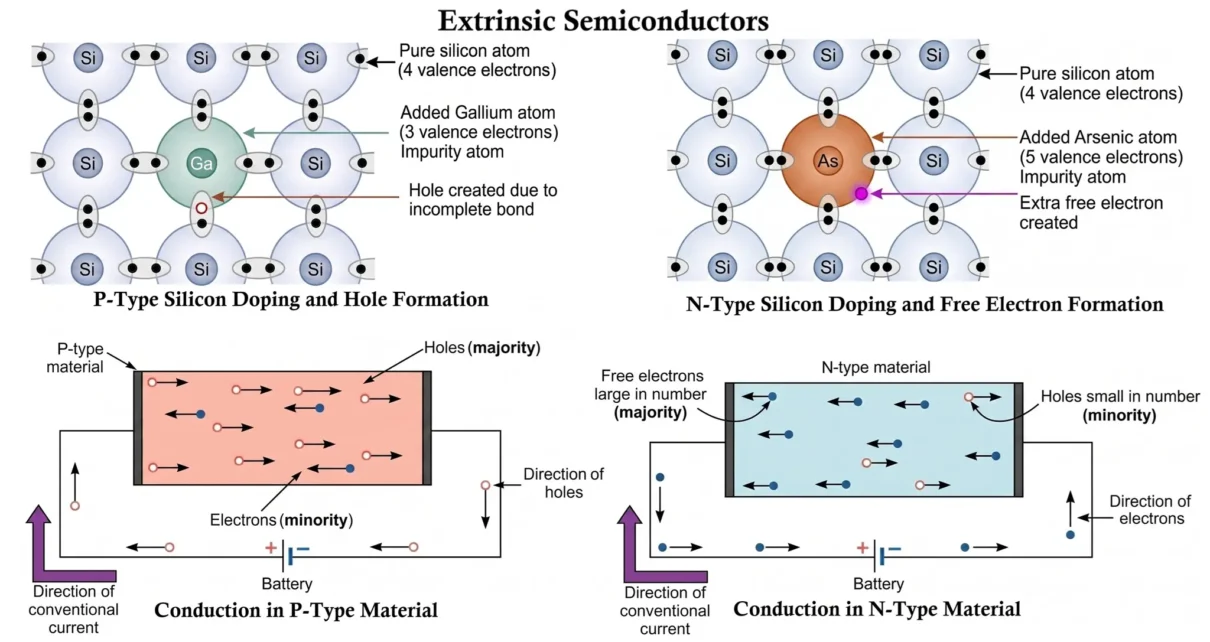
An n-type semiconductor is formed by adding a small amount of pentavalent impurity to a pure semiconductor crystal. The added impurity provides a large number of free electrons for conduction.
Formation of N-Type Semiconductor
Consider silicon doped with phosphorus or arsenic. Silicon has four valence electrons and forms four covalent bonds with neighboring atoms. A pentavalent impurity atom has five valence electrons.

- Out of these five electrons:
- Four electrons form covalent bonds
- One electron remains loosely bound
This extra electron becomes a free electron and contributes to electrical conduction.
Energy Band Diagram of N-Type Semiconductor
In n-type semiconductors, donor energy levels are introduced just below the conduction band. The small energy gap allows electrons to move easily into the conduction band.
- Important Features:
- Large number of free electrons
- Electrons are majority carriers
- Holes are minority carriers
- Conductivity increases greatly
Charge Carriers in N-Type Semiconductor
| Charge Carrier | Status |
|---|---|
| Electrons | Majority Carriers |
| Holes | Minority Carriers |
Conduction in N-Type Semiconductor
- When an external voltage is applied:
- Free electrons move toward the positive terminal
- Electron flow constitutes electric current
- Conduction mainly occurs due to electrons
Since electron concentration is very high, electron current dominates over hole current.

N-Type Semiconductor Formula
The conductivity of a semiconductor is:
σ = q(nμn + pμp)
- σ = Conductivity
- q = Electronic charge
- n = Electron concentration
- p = Hole concentration
- nμn = Electron mobility
- pμp = Hole mobility
For n-type semiconductors n >> p
Hence:
σ ≈ qnμn
Properties of N-Type Semiconductor
- High electron concentration
- Low hole concentration
- Conductivity mainly due to electrons
- Contains donor impurity atoms
- Electrically neutral overall
- Lower resistivity than intrinsic semiconductor
Advantages of N-Type Semiconductor
- Has high electrical conductivity due to the large number of free electrons.
- Electrons move faster than holes, resulting in better current flow.
- Requires less energy for conduction.
- Shows better performance at lower temperatures.
- Suitable for making high-speed electronic devices.
- Has lower resistance compared to intrinsic semiconductors.
Disadvantages of N-Type Semiconductor
- Minority carriers (holes) are very few, which may limit certain applications.
- Conductivity can change significantly with temperature.
- Excess doping may reduce semiconductor efficiency.
- Impurity atoms can introduce crystal defects in the material.
- More sensitive to contamination during manufacturing.
Applications of N-Type Semiconductor
- Used in the manufacture of diodes and transistors.
- Widely used in integrated circuits (ICs).
- Used in solar cells and photovoltaic devices.
- Applied in rectifiers and switching circuits.
- Used in computer microprocessors and digital electronics.
- Important in the fabrication of PN junction devices.
- Used in sensors and communication systems.
P-Type Semiconductor
A p-type semiconductor is formed by adding a small amount of trivalent impurity to a pure semiconductor crystal. The impurity creates holes that participate in conduction.
Formation of P-Type Semiconductor
Consider silicon doped with boron or gallium. The trivalent impurity atom has only three valence electrons. During covalent bonding three bonds are completed and one bond remains incomplete, this incomplete bond creates a hole.

A neighboring electron can move into this hole, causing the hole to shift position.
Energy Band Diagram of P-Type Semiconductor
In p-type semiconductors, acceptor energy levels are introduced just above the valence band. Electrons can easily move from the valence band into acceptor levels, creating holes.
- Important Features:
- Large number of holes
- Holes are majority carriers
- Electrons are minority carriers
- Conduction mainly due to holes
Charge Carriers in P-Type Semiconductor
| Charge Carrier | Status |
|---|---|
| Holes | Majority Carriers |
| Electrons | Minority Carriers |
Conduction in P-Type Semiconductor
- When voltage is applied:
- Holes move toward the negative terminal
- Electrons move in the opposite direction
- Hole current dominates conduction
Though electrons physically move, conventional current is considered in the direction of hole movement.

Formula for P-Type Semiconductor
For n-type semiconductors p >> n
Hence:
σ ≈ qpμp
- σ = Conductivity
- q = Electronic charge
- p = Hole concentration
- μp = Hole mobility
Properties of P-Type Semiconductor
- High hole concentration
- Low electron concentration
- Conduction mainly due to holes
- Contains acceptor impurities
- Lower resistivity than intrinsic semiconductor
Advantages of P-Type Semiconductor
- Has good electrical conductivity due to the presence of holes as majority carriers.
- Useful for forming PN junctions in electronic devices.
- Requires comparatively low energy for hole conduction.
- Plays an important role in controlling current flow in semiconductor devices.
- Suitable for use in amplifiers and switching circuits.
- Easy to combine with n-type materials to manufacture various electronic components.
Disadvantages of P-Type Semiconductor
- Hole mobility is lower than electron mobility, so conductivity is less than n-type semiconductors.
- Performance may decrease at high temperatures.
- Excessive doping can affect the crystal structure and efficiency.
- Minority carriers (electrons) are very few.
- More susceptible to recombination losses in some devices.
Applications of P-Type Semiconductor
- Used in the manufacture of PN junction diodes.
- Widely used in transistors and integrated circuits (ICs).
- Applied in LEDs and semiconductor lasers.
- Used in solar cells and photovoltaic systems.
- Important in rectifiers, amplifiers, and switching devices.
- Used in communication and signal-processing circuits.
- Forms an essential part of most modern electronic devices.
Extrinsic Semiconductor Energy Bands
Doping introduces new energy levels into the forbidden energy gap. The Fermi level changes after doping.
- N-Type
- Donor level lies close to conduction band
- Electrons easily move into conduction band
- P-Type
-
- Acceptor level lies close to valence band
- Holes are easily generated
-
- Fermi Level in Extrinsic Semiconductors
- N-Type Semiconductor: Fermi level shifts closer to conduction band
- P-Type Semiconductor: Fermi level shifts closer to valence band
Effect of Temperature on Extrinsic Semiconductors
- As temperature increases:
- More covalent bonds break
- More electron-hole pairs are generated
- Conductivity increases
At very high temperature, extrinsic semiconductors may behave like intrinsic semiconductors.
Difference Between Intrinsic and Extrinsic Semiconductor
| Feature | Intrinsic Semiconductor | Extrinsic Semiconductor |
|---|---|---|
| Purity | Pure semiconductor | Doped semiconductor |
| Conductivity | Low | High |
| Charge Carriers | Equal electrons and holes | Unequal carrier concentration |
| Impurity | No impurity | Impurity added |
| Carrier Type | Thermally generated | Due to doping |
| Applications | Limited | Widely used |
Difference Between N-Type and P-Type Semiconductor
| Feature | N-Type | P-Type |
|---|---|---|
| Dopant Type | Pentavalent | Trivalent |
| Majority Carrier | Electrons | Holes |
| Minority Carrier | Holes | Electrons |
| Impurity Type | Donor | Acceptor |
| Fermi Level | Near conduction band | Near valence band |
| Conductivity | Electron conduction | Hole conduction |
Advantages of Extrinsic Semiconductors
- High electrical conductivity compared to intrinsic semiconductors.
- Conductivity can be controlled through the doping process.
- Controlled carrier concentration improves device performance.
- Require less energy for current conduction.
- Support efficient current flow due to majority charge carriers.
- Improve the efficiency of semiconductor devices.
- Essential for the operation of modern semiconductor devices.
- Enable the development of miniaturized electronic circuits and components.
- Suitable for integrated circuits (ICs) and microprocessors.
- Effective in switching, amplification, and signal-processing applications.
Disadvantages of Extrinsic Semiconductors
- Sensitive to temperature changes, which can affect conductivity.
- Excessive doping may damage the crystal structure.
- Precise doping is required during manufacturing.
- Impurity concentration must be carefully controlled.
- Impurities may introduce crystal defects in the material.
- Fabrication process is complex and requires high purity materials.
- Leakage current may increase at high temperatures.
- More expensive to manufacture than intrinsic semiconductors.
Applications of Extrinsic Semiconductors
Extrinsic semiconductors are widely used in modern electronics because of their controlled conductivity and efficient charge carrier movement.
- Rectifier Diodes: Used to convert alternating current (AC) into direct current (DC).
- Zener Diodes: Used for voltage regulation and circuit protection.
- LEDs: Used in display panels, indicator lights, and lighting systems.
- Transistors: Used for amplification and switching in electronic circuits.
- MOSFETs: Used in high-speed switching and power electronics.
- Integrated Circuits (ICs): Used in computers, smartphones, calculators, and digital devices.
- Microprocessors and Microcontrollers: Used in computers, automation systems, and embedded devices.
- Solar Cells: Used to convert solar energy into electrical energy.
- Sensors: Used in temperature, pressure, light, and motion detection systems.
- Optoelectronic Devices: Used in photodiodes, laser diodes, and fiber optic communication.
- Communication Systems: Used in mobile phones, radio transmitters, and wireless networks.
- Medical Equipment: Used in diagnostic and monitoring instruments.
- Automotive Electronics: Used in engine control systems, electric vehicles, and safety devices.
Conclusion
Extrinsic semiconductors are semiconductor materials whose conductivity is improved through the process of doping. By adding pentavalent or trivalent impurities to pure silicon or germanium, n-type and p-type semiconductors are formed. In n-type materials, electrons are the majority carriers, while in p-type materials, holes dominate conduction.
The controlled conductivity, carrier concentration, and electrical characteristics of extrinsic semiconductors make them essential for modern electronic devices. From simple diodes to advanced microprocessors, almost every semiconductor device relies on the principles of extrinsic semiconductors.
Energy Band Theory of Solids: Conductors, Semiconductors, and Insulators
Types of Diodes: Symbol, Working, Characteristics and Applications
Types of Transistors: Classification (BJT, JFET, MOSFET & IGBT)
