RF and microwave PCB projects pass starting functional testing but face some performance instability for high-frequency validation, volume manufacturing, or long-term working features.
Common issues are:
- Excessive insertion loss
- Abnormal return loss
- Impedance mismatch
- Signal reflection
- EMI and crosstalk
- Ground discontinuity
- High-frequency loss caused by via transition
- RF performance drift after thermal cycling
The main challenges are RF microwave board design comes with different challenges than the digital PCB design does. An RF microwave board is not a circuit carrier that belongs to the RF signal transmission path. For the RF microwave board project, material selection, stack-up design, through-transition, impedance control, surface finish, and manufacturing tolerance should be checked once the layout is finalized, especially when working with an experienced high-frequency PCB manufacturer.
In HF frequency projects, small errors of geometry, dielectric features or grounding design can affect signal quality and RF functions. An advanced RF system requires close cooperation between PCB designers, RF engineers, and manufacturing teams from the earliest design phases.
Related Articles:
- PCB Manufacturing and Assembly Process
- High-Density Interconnect (HDI) PCB Manufacturing Process
- Types of PCB Materials Their Properties and Applications
- How to Assemble Electronic Components on a PCB
- Cost-Effective Overseas PCB Services for Small Businesses
- Revolutionary Axial Flux Printed Circuit Board (PCB) Stator Motor
- High Speed PCB Design: Routing, Impedance & Layout Techniques
- What are the Key Stages in Aluminum PCB Manufacturing?
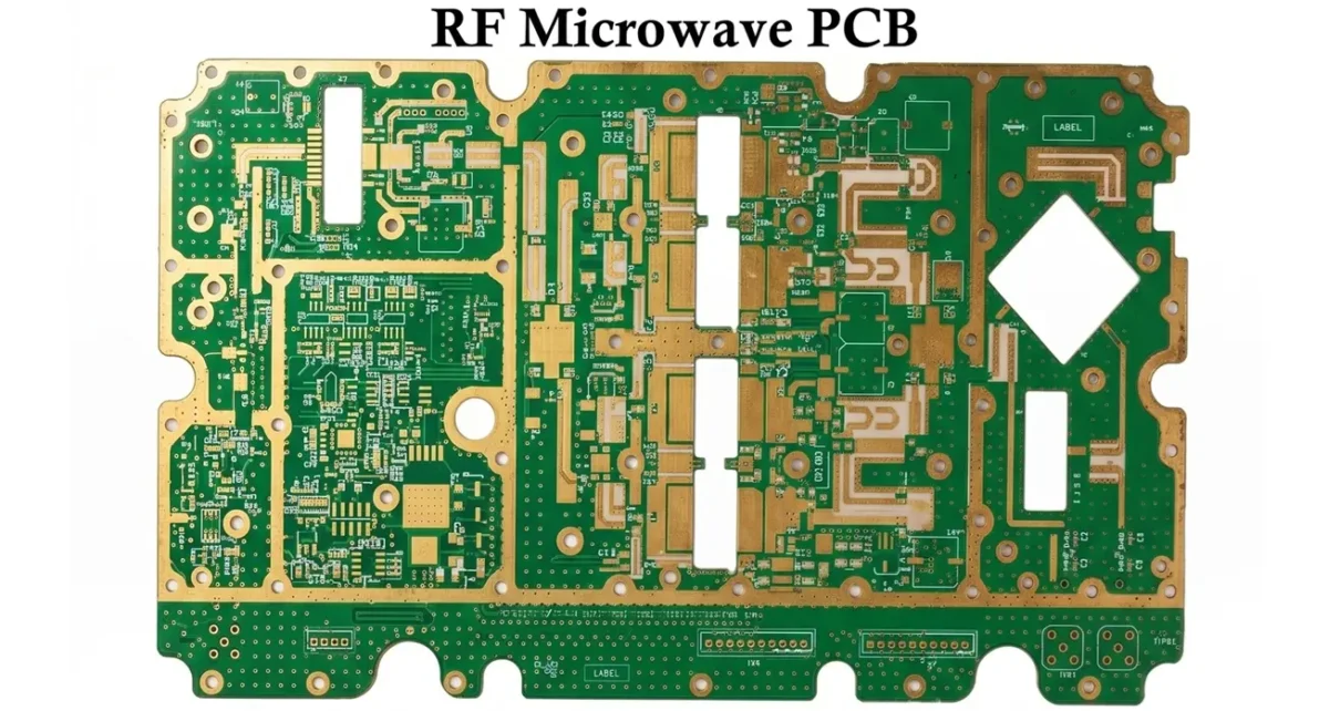
What Is an RF Microwave PCB?
An RF microwave board is normally designed for high-frequency signal transmission, normally more than 500MHz and often extending into multi-GHz applications. RF microwave PCBs are different from standard FR4 boards.
RF microwave PCB design works on:
- Stable dielectric constant (Dk)
- Low dissipation factor (Df)
- Controlled impedance
- Low transmission loss
- Ground continuity
- Precise manufacturing tolerances
These PCB technologies are commonly used in:
- 5G communication systems
- Automotive radar
- RF systems
- Satellite communication
- Aerospace electronics
- Test and measurement equipment
An RF microwave board is made for controlling signal features, not for connecting parts. Some advanced high-frequency projects needed special laminates and controlled manufacturing processes for stable electrical features over different functional conditions.
For further features of high-frequency board techniques and compatible RF materials, check the RF microwave board production features available from FastTurnPCB.
Material Selection
Material selection is the most important factor in RF microwave PCB design.
Dk and Df Importance
Dk (dielectric constant) affects:
- Signal propagation speed
- Controlled impedance
- Phase behavior
- Electrical field distribution
Df (dissipation factor) affects:
- Dielectric loss
- Insertion loss
- Heat generation at high frequency
As working frequency increases, low-Df materials become the main factor because dielectric loss rises fast in GHz-range applications. Material selection is the building block of RF microwave PCB performance since Dk and Df directly affect impedance, phase stability, and signal loss. With that, long-term Dk and Df stability under temperature changes, humidity exposure, and thermal cycling can affect RF consistency during field operation.
For different high-frequency systems more than 10 GHz, conductor losses and copper surface roughness are also main contributors to total insertion losses. So low-profile or ultra-low-profile copper foils are part of advanced RF stack-ups.
Common RF Microwave PCB Materials
Common high-frequency laminates are
- Rogers RO4003C
- Rogers RO4350B
- Rogers RO3003
- Rogers RO3010
- Rogers RT5880
- Taconic RF-35
- Taconic TLY-5
- Isola materials
- Nelco materials
- Panasonic Megtron series
- PTFE-based laminates
- Ceramic-filled materials
- Hybrid materials
Each material has certain features for loss performance, thermal stability, manufacturability, and cost.
For example:
- RO4350B is widely used for general RF applications with balanced cost and performance.
- RT5880 provides extremely low loss for microwave projects
- Ceramic-filled laminates have thermal and dimensional stability.
- Hybrid stack-ups combine RF materials with FR4 to optimize overall system cost.
Stack-up Design and Controlled Impedance
Stack-up design is the most important part of RF microwave PCB production. Most RF transmission lines are designed over a target impedance of 50Ω.
Getting stable impedance needs careful coordination of:
- Trace width
- Copper thickness
- Dielectric thickness
- Material Dk
- Reference plane structure
The stack-up should be finalized before PCB layout initiation. RF layers should maintain a continuous ground reference below the signal path to reduce impedance discontinuity and undesired radiation.
Hybrid stack-ups require additional consideration of:
- Material CTE compatibility
- Lamination stability
- Mechanical stress
- Impedance consistency across different laminate regions
Impedance mismatch causes signal reflection, high return loss, and RF performance degradation.
Correct impedance control often needs:
- Field solver simulation
- TDR verification
- Controlled etching compensation
- Manufacturing tolerance analysis
Small changes in the dielectric thickness or copper geometry can affect RF features significantly at microwave frequencies.
RF Layout Rules
RF layout quality affects insertion loss, EMI factor, and signal stability.
Recommended RF layout practices are:
- Keep RF traces short and direct
- Avoid sharp 90-degree corners
- Use 45-degree bends or curved traces
- Maintain a continuous ground plane
- Avoid ground splits under RF traces
- Separate RF circuits from noisy power or digital areas
- Use via stitching around RF paths when needed
- Avoid sudden trace width changes
- Confirm trace width using the actual production stack-up
In RF microwave PCB layout, every discontinuity can cause reflection, radiation, or signal loss.
Designers should also carefully handle:
- Return current paths
- RF connector transitions
- Shielding structures
- Ground via spacing
- Coupling between adjacent RF lines
accurate DFM review before manufacturing helps minimize the chances of impedance deviation and unexpected RF performance issues during manufacturing.
Via Design, Microvias, and Backdrilling
Importance of Vias in RF Microwave PCB
Vias are one of the largest hidden chance factors in high-frequency PCB performance.
Effects of adding via transition:
- Impedance discontinuity
- Parasitic inductance
- Parasitic capacitance
- Stub resonance effects
As operating frequency increases, parasitics become increasingly important. A faulty design via transition can affect RF performance; also, laminate and impedance calculations must be correct. In RF microwave PCB design, a stub is an unintended or intentional section of transmission line that is connected to the signal path but is not part of the desired signal route.
Through stubs can create unwanted resonance points that increase return loss, reflection, insertion loss and phase distortion.
Design Guidelines
Recommended RF via design features are:
- Minimize vias in RF signal paths
- Maintain continuous return paths during layer transitions
- Add nearby ground vias for RF transitions
- Optimize via pad and anti-pad geometry
- Use blind vias or microvias where appropriate
- Use backdrilling to reduce via stub effects
Laser drilling and mechanical drilling processes are commonly used for advanced RF microvia structures.
Backdrilling is particularly preferred for:
- High-speed RF transitions
- Multi-layer microwave designs
- GHz-range communication systems
- Backplane RF interconnects
For mmWave applications, more than 24 GHz, via optimization is very sensitive. Electromagnetic simulation is used to accurately model via transitions and resonance features.
Surface Finish Selection for RF Microwave PCB
Surface finish selection affects both assembly reliability and RF performance consistency.
Important considerations are:
- Solderability
- Surface flatness
- Contact reliability
- Corrosion resistance
- Assembly yield
High-frequency designs should prevent unnecessary surface roughness or uneven finishes that can affect conductor loss or RF contact features. RF contact areas often need tighter process control, since poor surface quality can affect long-term electrical stability.
Common surface finishes are:
- Immersion Gold
- OSP
- Hard Gold
- Immersion Silver
- ENEPIG
In RF microwave PCB manufacturing, surface finish, not assembly option, also affects RF contact reliability features and long-term manufacturing features. Fine-pitch RF components and microwave connectors are also important for highly planar and uniform surface finishes.
Manufacturing Capabilities and Process Control
The selection of an experienced high-frequency PCB manufacturer is important for maintaining stable RF performance throughout manufacturing.
A capable RF PCB supplier should support:
| Capability | Requirement |
| Materials | RO4003C, RO4350B, RO3003, RO3010, RT5880 |
| Min Track / Spacing | 3/3mil |
| Min Hole Size | 0.15mm |
| Finished Copper | 1-2oz |
| Board Thickness | 0.2-3.2mm |
| Surface Finish | Immersion Gold, OSP, Hard Gold, Immersion Silver, ENEPIG |
| Copper Capability | 0.5-13oz |
| Via Process | Tented vias, plugged vias, uncovered vias |
| Testing | Flying probe testing, AOI testing |
| Standard Build Time | 7-10 days |
| Quick-Turn Lead Time | 2-3 days |
Reliable RF PCB manufacturing needs:
- Controlled impedance processing
- TDR testing
- AOI inspection
- Etching compensation control
- Lamination process stability
- Tight drilling registration control
Early stack-up review and DFM analysis can significantly minimize yield faults and redesign cost in RF projects.
Reliability Risks and Failure Mechanisms
RF microwave PCB reliability based on the combined control of material, layout, stack-up, via design, surface finish, and manufacturing techniques
Common failure risks are:
- Impedance deviation
- Increased insertion loss
- Increased return loss
- Signal reflection
- Via stub resonance
- Delamination
- CTE mismatch
- Moisture-related Dk/Df drift
- Poor grounding
- Solder joint reliability issues
To improve long-term reliability, manufacturers commonly use:
- TDR testing
- Impedance coupons
- AOI inspection
- E-test
- Flying probe testing
IPC Class 2 and Class 3 process control standards are also frequently used for main RF applications.
Applications
5G and Wireless Communication
- Requires low-loss dielectric materials to minimize signal attenuation.
- Demands stable impedance control for consistent RF performance.
- Needs a continuous ground reference to maintain signal integrity.
- Relies on controlled phase performance for beamforming and high-speed data transmission.
- High-frequency signal quality directly impacts communication efficiency, coverage, and antenna performance.
Automotive Radar and ADAS
- Uses 24 GHz and 77 GHz radar systems for sensing and object detection.
- Requires stable dielectric constant (Dk) performance across operating conditions.
- Demands precise via transition design to minimize RF discontinuities.
- Needs tight fabrication tolerances for accurate radar operation.
- Requires excellent thermal reliability for long-term performance in harsh automotive environments.
- Even small impedance variations can reduce radar accuracy and detection reliability.
Aerospace and Satellite Communication
- Requires long-term RF stability over extended mission lifetimes.
- Demands low insertion loss to maximize signal transmission efficiency.
- Needs high manufacturing reliability to ensure mission-critical performance.
- Requires environmental durability against temperature extremes, vibration, humidity, and radiation.
- Relies on consistent RF performance at microwave and millimeter-wave frequencies.
- Supports high-reliability communication links for aerospace, defense, and satellite applications.
- These applications often function under severe thermal cycling conditions.
Medical and Industrial RF Equipment
- Requires stable signal transmission for accurate and reliable system operation.
- Demands high assembly quality to ensure consistent RF performance.
- Needs long operational lifetime under continuous use.
- Requires consistent RF characteristics throughout the product lifecycle.
- Supports applications where reliability and repeatability are critical.
RF Test and Measurement Equipment
- In RF test systems, the PCB is part of the measurement signal path.
- Requires low insertion loss to preserve signal accuracy.
- Demands excellent return loss for accurate impedance matching.
- Needs high phase stability to maintain measurement precision.
- Requires high-quality connector-to-PCB transitions to minimize RF discontinuities.
- Even small PCB imperfections can directly impact measurement accuracy and repeatability.
Cost Engineering and Optimization
Main Cost Drivers
Major RF microwave PCB cost drivers are:
- RF laminate pricing
- Rogers, Taconic, and PTFE utilization
- Controlled impedance requirements
- Tight etching tolerance
- Hybrid stack-up complexity
- Microvia and backdrilling processes
- Surface finish selection
- Testing requirements
- Yield risk
Optimization
Cost optimization strategies are:
- Avoid using expensive RF materials across the complete board unnecessarily
- Use hybrid stack-ups where appropriate
- Reduce unnecessary RF layer count
- Minimize via transitions in RF paths
- Confirm stack-up and impedance before layout
- Perform early DFM review
- choosing materials based on actual frequency and loss budget demand
The low PCB unit cost is not always the low project cost for RF and microwave projects. Poor material selection or weak process control can increase redesign cost, qualification delay, and field reliability faults.
Conclusion
Most RF microwave PCB faults do not occur from a single error but from a lack of integration between material selection, via transition, surface finish, stack-up design, impedance control, layout, and manufacturing process.
As operating frequencies continue moving rapidly into the GHz range, successful RF PCB production is increasingly based on early engineering collaboration and manufacturing-aware design decisions.
FastTurn PCB supports RF, microwave, and high-frequency PCB projects with material selection methods, stack-up review, impedance control, microvia and backdrilling features, PCB manufacturing, assembly, and testing support.
High Speed PCB Design: Essential Wiring Techniques for Optimal Performance
Revolutionary Axial Flux Printed Circuit Board (PCB) Stator Motor
