The P-Channel Metal Oxide Semiconductor Field Effect Transistor (MOSFET) is an essential semiconductor device widely used in electronic circuits, particularly in high-side switching and complementary configurations. Like other MOSFETs, it belongs to the family of field-effect transistors (FETs), where current conduction is controlled by an electric field rather than by direct current injection, as in bipolar junction transistors (BJTs). Because of this operating mechanism, MOSFETs are classified as voltage-controlled devices.
In a P-channel MOSFET, the conduction mechanism is fundamentally different from its N-channel counterpart. It uses holes as majority charge carriers, which move from source to drain under the influence of an electric field. Although hole mobility is lower than electron mobility, P-channel MOSFETs play a critical role in circuit design due to their unique electrical characteristics and ease of integration in certain configurations.
Compared to N-channel devices, P-channel MOSFETs typically exhibit:
- Higher ON resistance RDS(on)
- Slower switching speed
- Slightly lower efficiency in high-power applications
However, these limitations do not reduce their importance. Instead, P-channel MOSFETs are preferred in applications where simplified gate driving and high-side switching are required.
One of the major advantages of P-channel MOSFETs is that they can be easily driven without requiring complex gate driver circuits, especially in high-side configurations. This simplifies circuit design and reduces component count.
Similar to N-channel devices, P-channel MOSFETs also have extremely high input impedance due to their insulated gate structure. This ensures:
- Negligible gate current
- Minimal loading effect on previous stages
- Efficient operation in sensitive electronic systems
Symbol of P-Channel MOSFET
The symbol of a P-Channel MOSFET visually represents its structure, terminals, and mode of operation. Understanding this symbol is crucial for circuit design, analysis, and troubleshooting.

Terminals of P-Channel MOSFET
A P-channel MOSFET is fundamentally a four-terminal device, consisting of:
Gate (G): The control terminal that regulates the current flow. It is insulated from the channel by a thin oxide layer, resulting in almost zero gate current.
Drain (D): The terminal through which holes leave the channel. It is usually connected to a lower potential compared to the source.
Source (S): The terminal through which holes enter the channel. It is typically connected to a higher potential and serves as the reference for gate voltage.
Body (B) / Substrate: The semiconductor base material. In most practical MOSFETs, this terminal is internally connected to the source, so it is not shown separately in circuit diagrams.
Arrow Direction
A key identifying feature of the MOSFET symbol is the arrow direction, which indicates the type of channel and charge carriers.
- In a P-Channel MOSFET, the arrow points inward (toward the body/source)
- This indicates that conduction is due to holes (positive charge carriers)
- It also reflects the device’s polarity and operating behavior
This convention is based on the direction of conventional current flow across the body junction.
Enhancement Mode vs Depletion Mode Symbol
P-channel MOSFETs are classified based on their default operating condition:
Enhancement Mode P-Channel MOSFET
- Represented by a broken (dashed) channel line
- Device is normally OFF when VGS = 0
- Requires a negative gate voltage (with respect to source) to turn ON
- Most commonly used in practical applications
Depletion Mode P-Channel MOSFET
- Represented by a solid channel line
- Device is normally ON at zero gate voltage
- Gate voltage is used to reduce or increase conduction
Body Diode Representation
In many practical and power MOSFET symbols, an intrinsic body diode is shown between the drain and source.
- This diode:
- Is formed naturally due to the internal PN junction structure
- Plays an important role in switching applications
- Allows reverse current flow under specific conditions
- Is particularly significant in power electronics and protection circuits
Observations from the Symbol
From the P-channel MOSFET symbol, several key points can be understood:
- The insulated gate indicates very high input impedance
- The inward arrow confirms P-channel operation
- The channel line (solid or dashed) identifies depletion or enhancement mode
- The body terminal is usually tied to the source, simplifying it to a three-terminal device
A proper understanding of the P-channel MOSFET symbol allows engineers to quickly identify device type, predict its behavior, and design efficient and reliable electronic circuits.
Related Articles:
- MOSFET: Metal Oxide Semiconductor Field Effect Transistor
- N-Channel MOSFET: Symbol, Construction, Working & Applications
- MOS Capacitor and MOS Capacitance CV Curves Explained
- Difference Between D-MOSFET and E-MOSFET Explained
- JFET Junction Field Effect Transistors Working and Applications
- Bipolar Junction Transistors (BJT) Working and Applications
- IGBT Full Form, Symbol, Construction, Working and Applications
- Types of Transistors: Classification (BJT, JFET, MOSFET & IGBT)
Types of P-Channel MOSFET
P-Channel MOSFETs are primarily classified based on their mode of operation, which determines whether the device is naturally ON or OFF at zero gate voltage. This classification is crucial because it directly affects circuit behavior, biasing conditions, and the choice of application.
Enhancement-Mode P-Channel MOSFET (E-MOSFET)
The enhancement-type PMOS is the most commonly used P-channel MOSFET in practical electronic circuits, especially in CMOS and switching applications.

Key Characteristics:
- Device is normally OFF when VGS = 0
- No physical channel exists initially
- A negative gate voltage (with respect to source) is required to form a channel
- Conduction begins only when: VGS < VTH (negative threshold voltage)
Operational Insight:
When a negative voltage is applied to the gate:
- The electric field attracts holes toward the gate oxide interface
- This creates an inversion layer (P-type channel) between source and drain
- As |VGS| increases, the channel becomes more conductive
- Current flows from source to drain due to hole movement
Applications:
- CMOS logic circuits (as pull-up devices)
- High-side switching circuits
- Load switching in battery-operated systems
- Power management circuits
Why It Is Widely Used:
- No conduction at zero bias → low standby power loss
- Simple gate drive for high-side switching
- Essential for complementary operation with NMOS in CMOS
Depletion-Mode P-Channel MOSFET (D-MOSFET)
The depletion-type PMOS operates in a manner opposite to enhancement devices and is less commonly used.

Key Characteristics:
- Device is normally ON when VGS = 0
- A conductive P-type channel is already present
- Applying positive gate voltage reduces channel conductivity
Operational Insight:
- At VGS = 0, current flows freely due to the existing channel
- Applying positive gate voltage:
- Repels holes away from the channel
- Reduces channel width → decreases current
- Applying negative gate voltage:
- Enhances hole concentration
- Increases conductivity further
Applications:
- Analog circuits
- Constant current sources
- Active loads in amplifier circuits
- Specialized biasing networks
- Less common than enhancement-type MOSFETs
- Used in circuits where default conduction is required
Summary of P-Channel MOSFET Types
| Type | Default State | Key Behavior |
|---|---|---|
| Enhancement Mode | OFF | Requires negative gate voltage to conduct |
| Depletion Mode | ON | Gate voltage reduces conduction |
In modern electronics, enhancement-mode P-channel MOSFETs dominate due to their compatibility with CMOS technology, predictable switching behavior, and suitability for low-power and integrated circuit applications.
In CMOS (Complementary MOS) technology, P-channel MOSFETs work alongside N-channel MOSFETs to create highly efficient, low-power, and compact integrated circuits. Their complementary behavior is fundamental to the operation of digital logic systems.
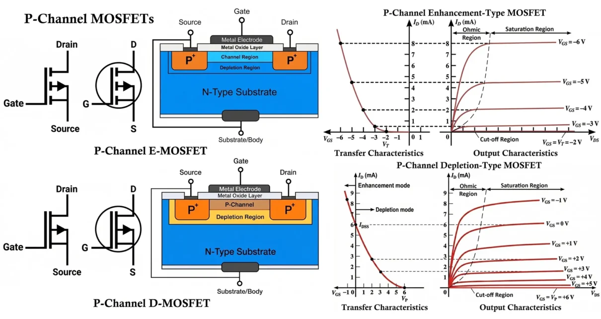
Construction and Structure of P-Channel MOSFETs
The construction of a P-Channel MOSFET is based on advanced semiconductor fabrication processes such as doping, oxidation, and thin-film deposition. Its internal structure is precisely engineered to control current flow using an electric field, which is the fundamental operating principle of all field-effect transistors.
Semiconductor Structure
A P-channel MOSFET is fabricated on an N-type semiconductor substrate, also referred to as the body (bulk) of the device. This substrate forms the base upon which the transistor structure is built.

- Within this N-type substrate:
- Two heavily doped P-type (P⁺) regions are formed
- These regions act as the Source (S) and Drain (D) terminals
Depending on the MOSFET type:
- Enhancement Mode (E-MOSFET): The region between source and drain is initially non-conductive, as it lacks holes
- Depletion Mode (D-MOSFET): A pre-existing P-type channel is already present, making the device naturally conductive
This intermediate region is known as the channel region, and its conductivity is externally controlled by the gate voltage.
Gate Oxide Layer (SiO₂)
A very thin insulating layer of silicon dioxide (SiO₂) is grown over the channel region through a thermal oxidation process. This layer is one of the most critical elements in MOSFET construction.
Functions of the Oxide Layer:
- Provides electrical insulation between gate and substrate
- Prevents direct current flow into the gate
- Enables electric field-based control of the channel
The oxide thickness is extremely small (typically in the nanometer range), allowing strong capacitive coupling while maintaining excellent insulation.
The quality of this layer directly impacts:
- Leakage current
- Breakdown voltage
- Overall device reliability
Gate Terminal Formation
A conductive material is deposited over the oxide layer to form the Gate (G) terminal. This material can be:
- Metal (used in early MOSFET technologies)
- Polysilicon (widely used in modern fabrication)
This arrangement of gate–oxide–substrate forms a structure equivalent to a capacitor, known as a MOS capacitor.
MOS Capacitor Concept
The MOSFET inherently behaves like a capacitor:
- Gate → one plate
- Substrate → second plate
- SiO₂ → dielectric medium

When a voltage VGS is applied between gate and source:
- An electric field is established across the oxide layer
- This field penetrates into the substrate
- It modifies the charge distribution in the channel region
This capacitive effect is the core mechanism that allows MOSFET operation without any direct electrical conduction through the gate.
Channel Formation and Field Control
A defining characteristic of MOSFET operation is:
- There is no direct conductive path between gate and channel
- The gate controls current purely via an electric field
In a P-channel MOSFET, when a negative gate voltage is applied (with respect to source):
- Holes (majority carriers) are attracted toward the oxide-substrate interface
- Electrons in the N-type substrate are repelled
- A thin layer rich in holes forms, known as the inversion layer
Once this inversion layer is established:
- A conductive channel connects source and drain
- Current flows when a voltage is applied between drain and source
This explains why the device is termed a Field-Effect Transistor (FET), its operation depends entirely on an electric field rather than charge injection.
Structural Insights
- Source and Drain Symmetry: Physically similar in construction, but their roles depend on circuit biasing
- Body Connection: In most practical devices, the body is internally connected to the source
- Oxide Layer Importance: Thickness and quality determine switching speed, leakage current, and long-term reliability
Advanced Structures
Modern P-channel MOSFETs incorporate advanced fabrication technologies such as:
- High-k dielectric materials (to reduce leakage and improve capacitance)
- FinFET (3D structures) for better electrostatic control
- Nanometer-scale fabrication for high-density integration
These innovations improve:
- Switching efficiency
- Power handling capability
- Scalability for integrated circuits
The carefully engineered structure of the P-channel MOSFET enables high input impedance, reliable operation, and effective control of current flow, making it an essential component in analog, digital, and power electronic systems, especially in complementary configurations like CMOS.
Working of P-Channel MOSFET (Enhancement Type)
The operation of a P-Channel Enhancement Type MOSFET (PMOS) is governed by the electric field effect, where the gate voltage controls the formation and conductivity of a channel between the source and drain. Unlike current-controlled devices, this mechanism relies entirely on electrostatic control of charge carriers (holes).

Cut-off Region (Initial Condition)
When no gate voltage is applied: VGS = 0
- No electric field exists across the oxide layer
- No inversion layer is formed
- The channel region remains non-conductive
- No drain current flows
- The MOSFET behaves like an open switch
This state is known as the cut-off region.
Channel Formation and Threshold Voltage
When a negative gate voltage is applied (with respect to source):
- An electric field is established across the SiO₂ layer
- Electrons in the N-type substrate are repelled
- Holes are attracted toward the oxide interface
As VGS becomes more negative, holes accumulate and form a thin conductive layer called the inversion layer (P-channel).
Threshold Condition:
VGS ≤ VTH,VTH is negative for PMOS
- VGS > VTH → Device OFF
- VGS ≤ VTH → Channel forms, device ON
Drain Current Flow
Once the channel is formed and a drain voltage is applied, VDS < 0 (Drain is at lower potential than source)
- Holes flow: Source → Drain
- Conventional current: Source → Drain
The drain current ID depends on gate voltage VGS and drain voltage VDS
Modes of Operation
Linear Region (Ohmic Region)
Condition: VGS < VTH and |VDS| << |VGS − VTH|
Drain Current Equation:
ID = p Cox (W/L) [ (VGS − VTH)VDS − (VDS² / 2) ]
- Behavior:
- Channel is fully formed
- MOSFET behaves like a voltage-controlled resistor
- Current varies approximately linearly with VDS
- Channel resistance decreases as |VGS| increases
Saturation Region (Active Region)
Condition: |VDS| ≥ |VGS − VTH|
Drain Current Equation:
ID = (1/2) p Cox (W/L) (VGS − VTH)²
- Behavior:
- Channel near the drain becomes pinched off
- Drain current becomes nearly constant
- ID depends mainly on VGS, not on VDS
- Used in analog amplification circuits
Pinch-Off Phenomenon
- As |VDS| increases:
- Voltage drop along the channel increases
- Channel width reduces near the drain end
- At a critical point → pinch-off occurs
Even after pinch-off:
- Current does not stop
- Holes continue to flow due to a strong electric field
- This results in a constant current region (saturation)
The P-channel MOSFET is a voltage-controlled current device, where the gate voltage controls channel formation, channel thickness and drain current
Application-Based Operation Modes
- Digital Electronics
- Operates as a switch
- Cut-off → OFF
- Saturation → ON
- Analog Electronics
- Operates in the saturation region
- Used for signal amplification
- Power Electronics
- Operates in:
- Linear region → controlled conduction
- Switching mode → high efficiency
This completes the working section with correct P-channel physics, polarity, and operation behavior.
Characteristics of P-Channel MOSFETs
The electrical behavior of a P-Channel MOSFET, whether enhancement or depletion type, is described using two fundamental characteristic curves:
- Output Characteristics: Relationship between drain current (ID) and drain-source voltage (VDS)
- Transfer Characteristics: Relationship between drain current (ID) and gate-source voltage (VGS)
These characteristics define how the MOSFET responds to applied voltages and are essential for biasing, design, and performance analysis in both analog and digital circuits.
Enhancement-Type P-Channel MOSFET
An enhancement-type PMOS operates by forming a channel only when a sufficient negative gate voltage is applied. At zero gate bias, the device remains OFF.

Output Characteristics (ID vs VDS)
These curves show how the drain current varies with drain voltage for different gate voltages.
Cut-off Region
Condition: VGS > VTH (less negative)
- Gate voltage is insufficient to form a channel
- No inversion layer exists
- Drain current is approximately zero
- Device behaves as an open switch
Linear (Ohmic) Region
Condition: VGS < VTH and |VDS| is small
Drain Current Equation:
ID = p Cox (W/L) [ (VGS − VTH)VDS − (VDS² / 2) ]
- Key Features:
- Channel is fully formed
- Current varies approximately linearly with VDS
- Device behaves as a voltage-controlled resistor
Saturation Region
Condition: |VDS| ≥ |VGS − VTH|
Drain Current Equation:
ID = (1/2) p Cox (W/L) (VGS − VTH)²
- Key Features:
- Channel is pinched off near drain
- Drain current becomes nearly constant
- Controlled mainly by VGS
- Used in amplifiers and analog circuits
Transfer Characteristics (ID vs VGS)
The transfer curve shows how drain current varies with gate voltage (typically in saturation).
- For VGS > VTH → ID ≈ 0 (device OFF)
- For VGS < VTH → ID ∝ (VGS − VTH)²
This quadratic relationship demonstrates that the MOSFET is a voltage-controlled current device.
Depletion-Type P-Channel MOSFET
Unlike enhancement devices, depletion-type PMOS has a pre-existing channel, so it conducts even at zero gate voltage.

Output Characteristics (ID vs VDS)
The shape of the curves is similar to enhancement MOSFETs but shifted due to the existing channel.
- At VGS = 0:
- Channel already exists
- Drain current is non-zero
Linear Region Equation:
ID = p Cox (W/L) [ (VGS − VTH)VDS − (VDS² / 2) ]
Saturation Region Equation:
ID = (1/2) p Cox (W/L) (VGS − VTH)²
- Effect of Gate Voltage:
- Positive VGS:
- Channel gets depleted
- Current decreases and may reach zero
- Negative VGS:
- Channel conductivity increases
- Current increases beyond zero-bias value
Transfer Characteristics (ID vs VGS)
The transfer curve extends across both positive and negative gate voltages.
Transfer Equation:
ID = IDSS (1 − VGS / VGS(off))²
- Behavior:
- At VGS = 0: Significant current flows
- As VGS becomes positive: Current decreases → device turns OFF
- As VGS becomes negative: Current increases further
This dual control makes depletion MOSFETs useful in analog applications.
Comparison E-MOSFET vs D-MOSFET
| Feature | Enhancement MOSFET | Depletion MOSFET |
|---|---|---|
| Channel at VGS = 0 | Absent | Present |
| Default State | OFF | ON |
| Gate Voltage Role | Creates channel | Modifies channel |
| Positive VGS | Keeps OFF | Reduces current |
| Negative VGS | Turns ON | Enhances conduction |
Important MOSFET Parameters
These parameters are derived from characteristic curves and are critical for circuit design.
- Threshold Voltage (VTH)
- Minimum gate voltage required for conduction
- Negative for PMOS
- Defines switching point
- Saturation Condition
- VDS = VGS − VTH
- Separates linear and saturation regions
- Pinch-Off Voltage (VP)
- Gate voltage where channel disappears
- For PMOS: typically positive (depletion type)
- Drain Current at Zero Gate Voltage (IDSS)
- Applicable to depletion MOSFETs
- Indicates natural conduction capability
- Transconductance (gm)
- gm = dID / dVGS
- Measures gain capability
- Higher gm → better amplification
- Drain-Source ON Resistance (RDS(on))
- Resistance when MOSFET is ON
- Lower value → higher efficiency
- Breakdown Voltage
- Maximum VDS before device failure
- Critical in power electronics
- Key Observations
- Enhancement vs Depletion → defines default ON/OFF behavior
- Gate voltage → controls current flow
- Operating region → determines application
This section maintains full technical parity while correctly adapting P-channel polarity, carrier physics, and equations.
Advantages of P-Channel MOSFET
Although P-channel MOSFETs have lower carrier mobility compared to N-channel devices, they offer several practical advantages that make them highly useful in specific circuit configurations.
- Simple Gate Drive for High-Side Switching
- One of the biggest advantages of PMOS is that it is easy to drive in high-side configurations.
- Source is usually connected to the supply voltage
- A negative gate voltage (relative to source) turns the device ON
- No need for complex bootstrap or charge pump circuits
- This makes PMOS ideal for power switching in battery-operated systems.
- Simplified Circuit Design
- Because of easier gate control:
- Fewer external components are required
- Circuit complexity is reduced
- Design becomes more reliable and compact
- High Input Impedance
- Like all MOSFETs:
- Gate is insulated by an oxide layer
- Negligible gate current flows
- Minimal loading on preceding stages
- This makes PMOS suitable for sensitive analog and logic circuits.
- Like all MOSFETs:
- Useful in Complementary Circuits (CMOS)
- P-channel MOSFETs are essential in CMOS (Complementary MOS) technology:
- PMOS acts as pull-up device
- NMOS acts as pull-down device
- Enables low power consumption and high noise immunity
- This combination forms the backbone of modern digital ICs and microprocessors.
- P-channel MOSFETs are essential in CMOS (Complementary MOS) technology:
- Efficient for Low-Voltage Applications
- PMOS devices perform well in:
- Battery-powered systems
- Portable electronics
- Low-voltage switching circuits
- Because they can be controlled easily without requiring higher gate voltages.
- PMOS devices perform well in:
- Intrinsic Reverse Polarity Protection
- In some configurations, the internal body diode of PMOS can be used advantageously:
- Protects circuits from reverse polarity
- Common in power input protection designs
Disadvantages of P-Channel MOSFET
Despite their advantages, P-channel MOSFETs have several limitations primarily due to the physical properties of charge carriers.
- Lower Hole Mobility
- PMOS uses holes as majority carriers, which have lower mobility than electrons.
- Results in slower switching speed
- Limits performance in high-frequency applications
- Higher ON Resistance (RDS(on))
- Due to lower mobility:
- PMOS has higher ON resistance than NMOS
- Leads to:
- Increased conduction losses
- More heat generation
- Reduced efficiency
- Lower Current Carrying Capability
- Compared to N-channel MOSFETs:
- PMOS devices handle less current for the same size
- Requires larger device size for equivalent performance
- Reduced Efficiency in Power Applications
- Higher resistance and slower switching result in:
- Increased power dissipation
- Lower efficiency in high-power circuits
- This makes PMOS less suitable for heavy-duty power electronics.
- Larger Silicon Area Requirement
- To compensate for lower mobility:
- PMOS devices need larger channel width (W)
- Increases chip area and cost in IC fabrication
- Gate Oxide Sensitivity
- Like all MOSFETs:
- Thin oxide layer is vulnerable to ESD
- Excessive gate voltage can damage the device
- Requires protective handling and circuit design
- Threshold Voltage Variability
- VTH varies with temperature and manufacturing process
- Can affect switching accuracy in precision circuits
- Body Diode Limitations
- The intrinsic diode can:
- Cause unwanted conduction paths
- Introduce reverse recovery losses in switching applications
- P-channel MOSFETs excel in simplicity and high-side switching
- N-channel MOSFETs dominate in efficiency and performance
Because of this, both are used together in complementary designs (CMOS) to achieve optimal performance.
Applications of P-Channel MOSFET
The P-Channel MOSFET (PMOS) is widely used in electronic circuits where simple control, high-side switching, and complementary operation are required. Although it is less efficient than N-channel MOSFETs in high-power applications, its design advantages make it essential in many practical systems.
High-Side Switching Applications
One of the most important applications of PMOS is high-side switching, where the load is connected to ground and the MOSFET is placed between the supply and the load.
- Source connected to supply voltage
- Gate driven below source voltage to turn ON
- No need for complex gate driver circuits
- Applications:
- Battery-powered devices
- Power distribution switches
- Load control circuits
PMOS is preferred here because it allows direct control using simple logic signals, unlike NMOS which requires a higher gate voltage than the supply.
Digital Electronics (CMOS Logic)
P-channel MOSFETs are fundamental in CMOS (Complementary MOS) technology, where they operate alongside N-channel MOSFETs.
- PMOS acts as pull-up network
- NMOS acts as pull-down network
- Applications:
- Logic gates (NOT, NAND, NOR)
- Microprocessors and microcontrollers
- Memory devices (RAM, ROM)
This complementary operation ensures:
- Low static power consumption
- High noise immunity
- Efficient switching performance
Power Management Circuits
PMOS devices are widely used in power management systems, especially where efficient and controlled power delivery is required.
- Applications:
- Voltage regulators
- Load switching circuits
- Power path control
- Useful in:
- Battery-powered electronics
- Portable devices
- Embedded systems
Reverse Polarity Protection
P-channel MOSFETs are commonly used in reverse polarity protection circuits.
- Acts as a smart diode
- Prevents damage if supply polarity is reversed
- Offers lower voltage drop compared to conventional diodes
- Applications:
- Power input protection
- Battery charging systems
- Automotive electronics
Analog Circuits and Active Loads
In analog electronics, PMOS transistors are used as:
- Active loads
- Current sources
- Applications:
- Differential amplifiers
- Operational amplifiers (op-amps)
- Biasing circuits
They typically operate in the saturation region, where current depends on:
ID ∝ (VGS − VTH)2
This allows predictable and stable analog behavior.
Switching Circuits
PMOS devices are used as electronic switches, especially where high-side control is required.
- They are preferred because:
- Require very low gate current
- Provide simple control logic
- Reduce need for additional driver stages
- Applications:
Battery and Portable Systems
PMOS is extensively used in battery-operated systems due to its easy gate drive requirements.
- They improve:
- Power efficiency
- System reliability
- Circuit simplicity
- Applications:
- Battery protection circuits
- Charging/discharging control
- Power gating in portable devices
Signal Routing and Multiplexing
PMOS transistors are used in analog switches and multiplexers.
- Signal routing circuits
- Analog multiplexers
- Sample-and-hold circuits
Often combined with NMOS to form transmission gates for better signal integrity.
Motor and Load Control (Limited Use)
While NMOS dominates motor control, PMOS is still used in:
- High-side control stages
- Low-power motor applications
- Applications:
- Small DC motor control
- Embedded control systems
- PMOS is preferred where simplicity and high-side control are critical
- NMOS is preferred where efficiency and high current capability are required
- Both are used together in CMOS systems for optimal performance
N-Channel MOSFET vs P-Channel MOSFET
MOSFETs are broadly classified into N-channel (NMOS) and P-channel (PMOS) devices based on the type of charge carriers involved. While both operate on the same electric field control principle, their electrical behavior, efficiency, and practical usage differ significantly.
Operational Condition
The turn-ON condition differs in polarity:
- NMOS: VGS > VTH
- PMOS: VGS < VTH (negative with respect to source)
- This means:
- NMOS requires a positive gate voltage
- PMOS requires a negative (or lower than source) gate voltage
Fundamental Difference
The key distinction lies in the charge carriers:
- N-Channel MOSFET: Electrons (negative carriers)
- P-Channel MOSFET: Holes (positive carriers)
Since electron mobility is higher, NMOS devices inherently provide better electrical performance.
- Carrier Mobility and Speed
- NMOS → Higher electron mobility → Faster switching
- PMOS → Lower hole mobility → Slower operation
- ON Resistance (RDS(on))
- NMOS → Lower resistance → less power loss
- PMOS → Higher resistance → more heat dissipation
- Current Carrying Capability
- NMOS → Handles higher current efficiently
- PMOS → Lower current capability for same size
- Switching Performance
- NMOS → Preferred for high-frequency switching
- PMOS → Used where speed is not critical
- Gate Driving Requirement
- NMOS → Easy for low-side switching
- PMOS → Ideal for high-side switching (no boosted gate required)
- Circuit Complexity
- NMOS → Needs driver circuits for high-side
- PMOS → Simplifies high-side design
- Power Efficiency
- NMOS → High efficiency
- PMOS → Moderate efficiency
Comparison: NMOS vs PMOS
| Parameter | N-Channel MOSFET (NMOS) | P-Channel MOSFET (PMOS) |
|---|---|---|
| Charge Carriers | Electrons | Holes |
| Mobility | High | Low |
| Switching Speed | Fast | Slower |
| ON Resistance | Low | High |
| Current Capability | High | Lower |
| Gate Voltage | VGS > VTH | VGS < VTH |
| Efficiency | High | Moderate |
| Typical Use | Power switching, digital circuits | High-side switching |
Application Preference
- NMOS is preferred in:
- Power electronics
- High-speed switching
- Digital ICs and processors
- PMOS is preferred in:
- High-side switching
- Load switching in battery systems
- Complementary circuits (CMOS)
Complementary Operation (CMOS Insight)
In modern electronics, NMOS and PMOS are rarely used in isolation. Instead, they are combined in CMOS technology:
- NMOS → Pull-down network
- PMOS → Pull-up network
- This combination provides:
- Very low power consumption
- High noise immunity
- Efficient digital switching
Conclusion
The P-Channel MOSFET plays a crucial role in modern electronics, particularly in applications requiring simple gate control and high-side switching. Although it exhibits lower performance compared to N-channel devices due to reduced carrier mobility, its ability to simplify circuit design makes it indispensable in many practical systems.
While N-channel MOSFETs dominate in terms of efficiency, speed, and current handling, P-channel MOSFETs remain essential for:
- Complementary operation in CMOS circuits
- Power management systems
- Battery-operated devices
- High-side switching applications
In real-world designs, engineers rarely choose between NMOS and PMOS in isolation. Instead, both are used together to achieve an optimal balance between performance, efficiency, simplicity and reliability.
A strong understanding of both device types enables better design decisions in power electronics, embedded systems, VLSI design, and analog circuits.
- Popular P-Channel MOSFET Examples
- Enhancement-Type PMOS: BS250, IRF9540, IRF4905, AO3407
- Depletion-Type PMOS: BSP149, DN2625, LND250
This concludes the comprehensive overview of P-channel MOSFETs, covering their working principles, characteristics, advantages, disadvantages, applications, and comparison with N-channel MOSFETs.
N-Channel MOSFETs: Symbol, Construction, Working, Characteristics and Applications
JFET Junction Field Effect Transistors Working and Applications
IGBT Full Form, Symbol, Construction, Working and Applications
