The N-Channel Metal Oxide Semiconductor Field Effect Transistor (MOSFET) is one of the most widely used semiconductor devices in modern electronics, particularly in switching and power applications. It belongs to the family of field-effect transistors (FETs), where the flow of current is controlled by an electric field rather than by charge injection, as seen in bipolar junction transistors (BJTs). Due to this operating principle, MOSFETs are classified as voltage-controlled devices.
Among all MOSFET types, the N-Channel MOSFET is especially significant because of its superior electrical performance. It uses electrons as majority charge carriers, which have higher mobility compared to holes in P-channel devices. This results in:
- Lower ON resistance RDS(on)
- Faster switching speed
- Higher efficiency in power applications
Because of these advantages, N-channel MOSFETs are extensively used in:
- Switch Mode Power Supplies (SMPS)
- DC motor drivers and control circuits
- Inverters and converters
- Digital logic circuits (especially CMOS technology)
- High-frequency switching applications
Another important feature is their extremely high input impedance, due to the insulated gate structure. This ensures negligible gate current and minimal loading on preceding stages, making them ideal for sensitive and high-speed electronic circuits.
In modern electronics, especially in integrated circuits, N-channel MOSFETs form a fundamental building block, enabling compact, efficient, and high-speed designs.
Related Articles:
- MOSFET: Metal Oxide Semiconductor Field Effect Transistor
- MOS Capacitor and MOS Capacitance CV Curves Explained
- Difference Between D-MOSFET and E-MOSFET Explained
- JFET Junction Field Effect Transistors Working and Applications
- Bipolar Junction Transistors (BJT) Working and Applications
- IGBT Full Form, Symbol, Construction, Working and Applications
- Types of Transistors: Classification (BJT, JFET, MOSFET & IGBT)
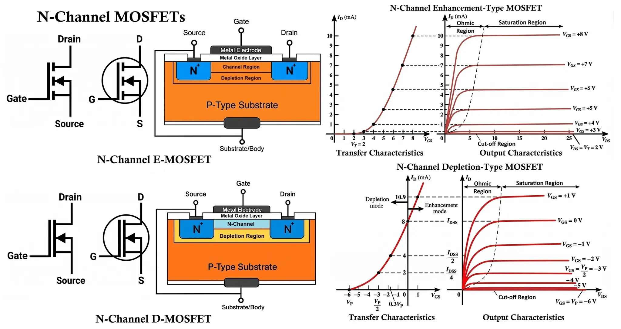
Symbol of N-Channel MOSFETs
The symbol of an N-Channel MOSFET is designed to clearly represent its terminals, structure, and mode of operation. Understanding this symbol is essential for circuit design, analysis, and troubleshooting.

Terminals of N-Channel MOSFET
An N-channel MOSFET is fundamentally a four-terminal device, consisting of:
- Gate (G): The control terminal that regulates current flow. It is insulated from the channel by a thin oxide layer, so it draws almost zero current.
- Drain (D): The terminal through which electrons leave the channel. It is usually connected to a higher potential.
- Source (S): The terminal through which electrons enter the channel. It often acts as the reference point for gate voltage.
- Body (B) / Substrate: The semiconductor base material. In most practical devices, this terminal is internally connected to the source, so it is not shown separately in circuit symbols.
Arrow Direction
A key identifying feature of the MOSFET symbol is the arrow direction, which indicates the type of channel.
- In an N-Channel MOSFET the arrow points outward (away from the body/source)
- This indicates that conduction is due to electrons (negative charge carriers)
- Device is optimized for high-speed and low-resistance switching
This convention is based on the direction of conventional current relative to the body junction.
For a P-Channel MOSFET, the arrow points inward (toward the body) and conduction occurs due to holes.
Enhancement Mode vs Depletion Mode Symbol
N-channel MOSFETs are further classified based on their default operating state:
- Enhancement Mode N-Channel MOSFET
- Represented by a broken (dashed) channel line
- Device is normally OFF when VGS = 0
- Requires a positive gate voltage to form a conductive channel
- Most commonly used in practical circuits
- Depletion Mode N-Channel MOSFET
- Represented by a solid channel line
- Device is normally ON at zero gate voltage
- Gate voltage is used to reduce or enhance conduction
Body Diode Representation
In many power MOSFET symbols, an intrinsic body diode is included between the drain and source. This diode:
- Is formed naturally due to the internal semiconductor structure
- Plays a crucial role in switching applications (like SMPS and motor drivers)
- Allows reverse current flow under certain conditions
Observations from the Symbol
- The gate is insulated, indicating no direct electrical connection to the channel
- The arrow direction confirms N-channel type
- The channel line (solid/dashed) indicates depletion or enhancement mode
- The body is usually tied to source, simplifying the symbol to three terminals
A clear understanding of the N-channel MOSFET symbol allows you instantly identify device type, predict its behavior in a circuit, and design efficient electronic systems.
Types of N-Channel MOSFET
N-Channel MOSFETs are primarily classified based on their mode of operation, which determines whether the device is naturally ON or OFF at zero gate voltage. This classification is critical because it directly influences circuit behavior, biasing requirements, and application domain.
Enhancement-Mode N-Channel MOSFET (E-MOSFET)
The enhancement-type NMOS is the most widely used MOSFET in practical electronics.

- Key Characteristics:
- Device is normally OFF when VGS = 0
- No physical channel exists initially
- A positive gate voltage is required to induce a channel
- Conduction begins only when: VGS > VTH
- Operational Insight:
- Gate voltage attracts electrons to form an inversion layer
- Channel conductivity increases with increasing ( VGS )
- Applications:
- Digital logic circuits (switching)
- Power electronics (SMPS, motor drivers)
- Microprocessors and integrated circuits
- Why It Dominates:
- Zero standby conduction → low power consumption
- Excellent switching speed
- High efficiency
Depletion-Mode N-Channel MOSFET (D-MOSFET)
The depletion-type NMOS operates in the opposite manner compared to enhancement devices.

- Key Characteristics:
- Device is normally ON when VGS = 0
- A conductive channel already exists
- Applying negative gate voltage reduces channel conductivity
- Operational Insight:
- Negative VGS → depletes electrons → reduces current
- Positive VGS → enhances conduction further
- Applications:
- Analog circuits
- Constant current sources
- Specialized amplifier circuits
- Note:
-
- Less common than enhancement MOSFETs
- Used where default conduction is required
-
N-channel MOSFETs are broadly classified based on mode of operation
| Type | Default State | Key Behavior |
|---|---|---|
| Enhancement Mode | OFF | Requires gate voltage to conduct |
| Depletion Mode | ON | Gate voltage reduces conduction |
In practical electronics, Enhancement-mode NMOS devices dominate due to their superior efficiency, scalability, and compatibility with modern integrated circuit design.
Construction and Structure of N-Channel MOSFETs
The construction of an N-Channel MOSFET is based on precise semiconductor fabrication techniques such as doping, oxidation, and thin-film deposition. Its internal structure is carefully engineered to enable control of current flow using an electric field, which is the defining principle of field-effect transistors.
Semiconductor Structure
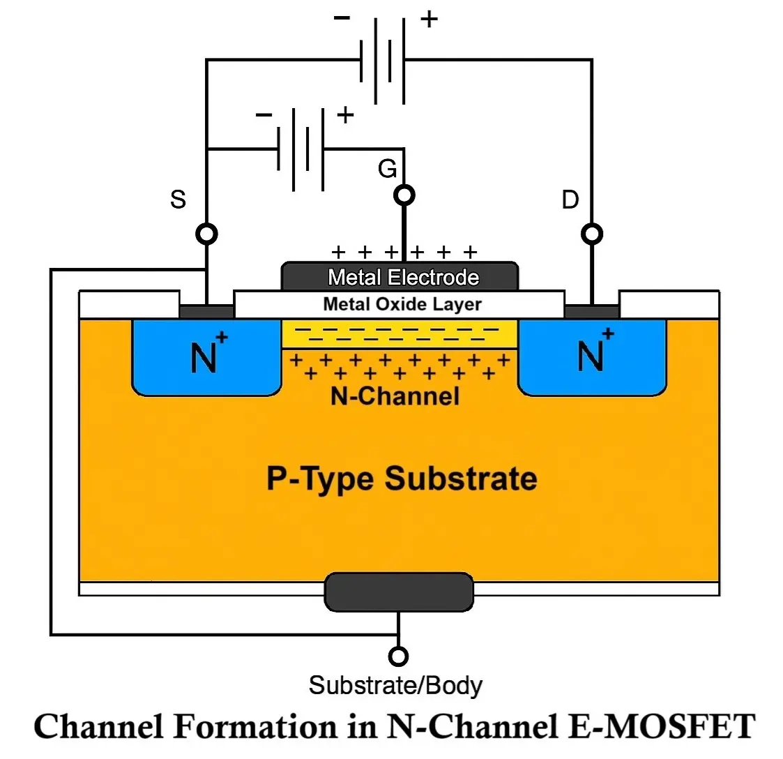
An N-channel MOSFET is fabricated on a P-type semiconductor substrate, also known as the body (bulk) of the device. This substrate acts as the foundational layer upon which the transistor is built.

- Within this P-type substrate:
- Two heavily doped N-type (N⁺) regions are created
- These regions form the Source (S) and Drain (D) terminals
- For E-MOSFET the region between them is initially non-conductive, as it lacks free electrons
- For D-MOSFET the region between them is initially conductive because n type channel is present
This intermediate region, known as the channel region, its conductivity is not permanent, it is controlled externally by the gate voltage. We will focus on enhancement type MOSFET and depletion type MOSFET can have similar structure with preexisting channel between source and drain terminal.
Gate Oxide Layer (SiO₂)
A very thin insulating layer of silicon dioxide (SiO₂) is formed over the channel region using a thermal oxidation process. This oxide layer is one of the most critical elements in MOSFET construction.
- Its primary functions include:
- Providing electrical insulation between the gate and substrate
- Preventing any direct current flow into the gate
- Enabling electric field-based control of the channel
The oxide thickness is extremely small (typically in the nanometer range), allowing strong capacitive coupling while maintaining insulation.
The quality of this layer directly affects leakage current, breakdown voltage and device reliability.
Gate Terminal Formation
On top of the SiO₂ layer, a conductive material is deposited to form the Gate (G) terminal. Depending on the fabrication technology, this material can be:
- Metal (used in early MOSFETs)
- Polysilicon (commonly used in modern devices)
This arrangement of gate, oxide, and substrate forms a structure analogous to a capacitor, commonly referred to as a MOS capacitor.
MOS Capacitor Concept
The MOSFET inherently behaves like a capacitor:
- Gate → one plate
- Substrate → second plate
- SiO₂ → dielectric medium
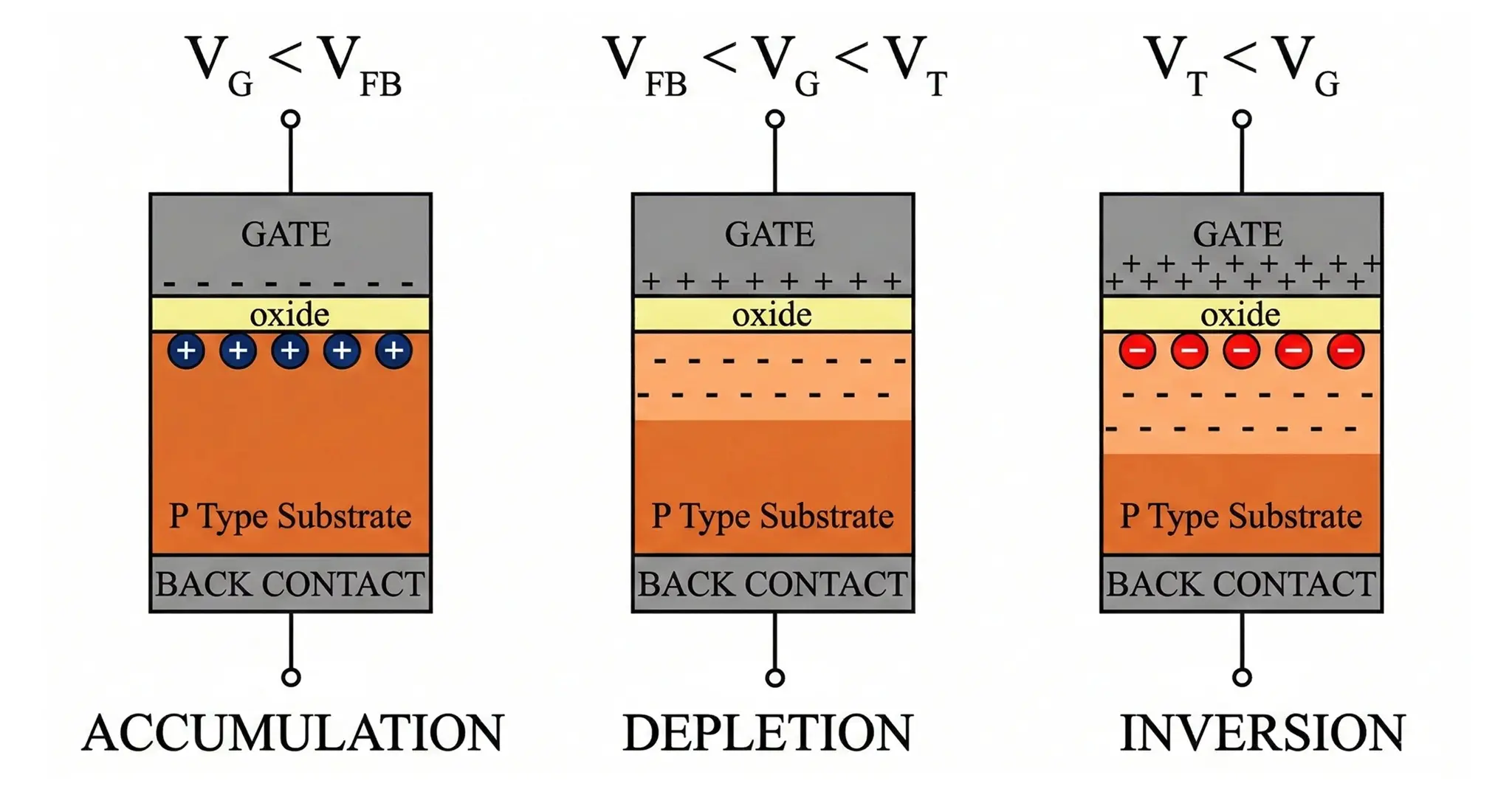
When a voltage VGS is applied between gate and source:
- An electric field is established across the oxide
- This field penetrates into the substrate
- It alters the charge distribution in the channel region
This capacitive behavior is the core mechanism that allows the MOSFET to operate without any direct electrical conduction through the gate.
Channel Formation and Field Control
A defining feature of MOSFET construction is that:
- There is no physical conductive connection between gate and channel
- The gate controls current purely via an electric field
When a positive gate voltage is applied in an N-channel MOSFET:
- Electrons (majority carriers) are attracted toward the oxide-substrate interface
- Holes in the P-type substrate are repelled
- A thin layer rich in electrons is formed, this is called the inversion layer
Once this inversion layer forms:
- A conductive channel connects the source and drain
- Current can flow when a voltage is applied across drain and source
This explains why the device is termed a Field-Effect Transistor (FET), its operation depends on an electric field rather than current injection.
Structural Insights
- Source and Drain Symmetry: Physically similar, but their roles depend on circuit biasing
- Body Connection: In most discrete MOSFETs, the body is internally connected to the source
- Oxide Layer Importance: Its thickness and quality determine switching performance, leakage, and durability
- Advanced Structures:
Modern devices use innovations such as:- High-k dielectric materials
- Fin-FET (3D structures)
- Ultra-scaled nanometer fabrication
- These advancements improve:
- Switching efficiency
- Power handling capability
- Device scaling for integrated circuits
The carefully engineered structure of the N-channel MOSFET enables very high input impedance, low power consumption and fast switching speeds. These characteristics make it indispensable in both power electronics and modern digital systems.
Working of N-Channel MOSFET (Enhancement Type)
The operation of an N-Channel Enhancement Type MOSFET is governed by the electric field effect, where the gate voltage controls the formation and conductivity of a channel between the source and drain. Unlike current-controlled devices, this mechanism relies entirely on electrostatic control of charge carriers (electrons).
Cut-off Region (Initial Condition)
When no gate voltage is applied: VGS = 0
- No electric field exists across the oxide layer
- No inversion layer is formed
- The channel region remains non-conductive
- This result in no drain current flows
- The MOSFET behaves like an open switch
This state is known as the cut-off region.
Channel Formation and Threshold Voltage
When a positive gate voltage is applied:
- An electric field develops across the SiO₂ layer
- Holes are repelled from the surface
- Electrons are attracted toward the interface
As VGS increases, electrons accumulate and form a thin conductive layer called the inversion layer.
Threshold Condition: VGS ≥ VTH
Threshold voltage VTH is the minimum gate voltage required to form a stable channel
- VGS < VTH → Device OFF
- VGS ≥ VTH → Channel forms, device ON
Drain Current Flow
Once the channel is formed and a drain voltage is applied: VDS > 0
- Electrons flow: Source → Drain
- Conventional current: Drain → Source
The drain current ID depends on gate voltage VGS and drain voltage VDS.
Modes of Operation
Linear Region (Ohmic Region)
- Condition: VGS > VTH and VDS ≪ (VGS – VTH)
Drain Current Equation:
ID = μn Cox (W/L) [ (VGS - VTH)VDS - (VDS2)/2 ]
Behavior:
- Channel is fully formed
- MOSFET behaves like a voltage-controlled resistor
- Current increases approximately linearly with ( VDS )
- Channel resistance decreases as ( VGS ) increases
Saturation Region (Active Region)
Condition: VDS ≥ (VGS – VTH)
Drain Current Equation:
ID = (1/2) μn Cox (W/L) (VGS - VTH)2
Behavior:
- Channel near drain gets pinched off
- Current becomes nearly constant
- ID depends mainly on VGS, not VDS
- Used in Amplifiers and analog circuits
Pinch-Off Phenomenon
As VDS increases:
- Voltage drop along the channel increases
- Channel width reduces near the drain
- At a critical point → pinch-off occurs
- Even after pinch-off current does not stop
Electrons continue flowing due to strong electric field, this results in a constant current region.
MOSFET is a voltage-controlled current device and gate voltage controls channel formation, channel thickness and drain current.
- Digital Electronics
- Operates as a switch
- Cut-off → OFF, Saturation → ON
- Analog Electronics
- Operates in saturation region
- Used for amplification
- Power Electronics
- Operates in Linear region (controlled conduction) and switching mode (high efficiency)
Characteristics of N-Channel MOSFETs
The electrical behavior of an N-Channel MOSFET, whether enhancement or depletion type, is described using two fundamental characteristic curves:
- Output Characteristics: Relationship between drain current (ID) and drain-source voltage VDS
- Transfer Characteristics: Relationship between drain current (ID) and gate-source voltage VGS
These curves define how the MOSFET responds to applied voltages and are essential for biasing, design, and performance analysis in both analog and digital circuits.
Enhancement-Type N-Channel MOSFET
An enhancement MOSFET operates by inducing a channel only when sufficient gate voltage is applied. At zero gate bias, the device remains OFF.

Output Characteristics (ID vs VDS)
The output characteristics describe how the drain current varies with drain voltage for different gate voltages.
Cut-off Region
Condition: VGS < VTH
In this region, the gate voltage is insufficient to form an inversion layer. As a result, no conducting channel exists between the drain and source.
- Drain current is approximately zero
- The device behaves as an open switch
Linear (Ohmic) Region
Condition: VGS > VTH, VDS is small
When the gate voltage exceeds the threshold, a conductive channel is formed. For small drain voltages, the device behaves like a controlled resistor.
Drain current equation:
ID = μn Cox (W/L) [(VGS - VTH)VDS - VDS2/2]
Key features:
- Current increases approximately linearly with VDS
- Channel is continuous and uniform
- Device acts as a voltage-controlled resistor
Saturation Region
Condition: VDS ≥ (VGS – VTH)
At higher drain voltages, the channel near the drain becomes pinched off. Beyond this point, further increases in VDS produce little change in current.
Drain current equation:
ID = 1/2 μn Cox W/L (VGS - VTH)2
Key features:
- Drain current becomes nearly constant
- Controlled primarily by VGS
- Suitable for amplification and current source applications
Transfer Characteristics (ID vs VGS)
The transfer characteristics illustrate how the drain current responds to changes in gate voltage (typically in saturation).
- For VGS < VTH: ID ≈ 0 (device OFF)
- For VGS > VTH: ID ∝ (VGS – VTH)2
This quadratic relationship highlights the strong control of gate voltage over the drain current, making the MOSFET an efficient voltage-controlled current device.
Depletion-Type N-Channel MOSFET
Unlike enhancement devices, depletion MOSFETs have a pre-existing channel. Therefore, they conduct even when no gate voltage is applied.

Output Characteristics (ID vs VDS)
The general shape of the output curves resembles that of the enhancement MOSFET but is shifted due to the presence of an already-formed channel.
Key Observations:
-
- At VGS = 0:
- A conducting channel already exists
- Drain current is non-zero
- At VGS = 0:
Drain current equation (Linear Region):
ID = μn Cox (W/L) [(VGS - VTH)VDS - VDS2/2]
Drain current equation (Saturation Region):
ID = 1/2 μn Cox (W/L) (VGS - VTH)2
- For negative VGS:
- The channel is depleted of carriers
- Drain current decreases and can reach zero
- For positive VGS:
- Channel conductivity increases further
- Drain current increases beyond its zero-bias value
Transfer Characteristics (ID vs VGS)
The transfer curve of a depletion MOSFET extends across both negative and positive gate voltages.
Transfer equation:
ID = IDSS (1 - VGS / VGS(off))2
- At VGS = 0:
- Significant drain current flows
- As VGS becomes negative:
- Current decreases gradually
- Device eventually turns OFF
- As VGS becomes positive:
- Current increases further
This bidirectional control makes depletion MOSFETs versatile for certain analog applications.
Comparison E-MOSFET vs D-MOSFET
| Feature | Enhancement MOSFET | Depletion MOSFET |
|---|---|---|
| Channel at VGS = 0 | Absent | Present |
| Default state | OFF | ON |
| Gate voltage role | Creates channel | Modifies channel |
| Negative VGS | No conduction | Reduces current |
| Positive VGS | Enables conduction | Enhances conduction |
Enhancement and depletion MOSFETs differ fundamentally in their channel formation and operating behavior. While enhancement MOSFETs require a gate voltage to initiate conduction, depletion MOSFETs conduct by default and allow both enhancement and depletion of current through gate control. Understanding these characteristics is essential for designing amplifiers, switches, and analog circuits.
Important MOSFET Parameters
These parameters are extracted from characteristic curves and are critical for design.
Threshold Voltage VTH
- Minimum gate voltage to start conduction
- Typical: 1V – 4V
- Defines switching point
- Saturation Condition: VDS = VGS – VTH
- Separates linear and saturation regions
Pinch-Off Voltage VP
- Gate voltage where channel fully disappears
- For NMOS: typically negative (depletion type)
Drain Current at Zero Gate Voltage
IDSS (for depletion MOSFET)
Indicates natural conduction capability
Transconductance
gm = dID / dVGS
- Measures gain capability
- Higher ( gm ) → better amplification
Drain-Source ON Resistance
RDS(on)
- Resistance when MOSFET is ON
- Lower value → higher efficiency
Breakdown Voltage
- Maximum VDS before failure
- Critical in power applications
The characteristic curves clearly show:
- Enhancement vs Depletion → default ON/OFF behavior
- Voltage control → governs current flow
- Region of operation → defines application role
This deep understanding of characteristics is essential for accurate circuit design, efficient biasing and high-performance electronic systems.
Advantages of N-Channel MOSFET
- High Electron Mobility: The NMOS uses electrons as majority carriers, which have significantly higher mobility than holes. This directly results in faster switching speeds, making the device ideal for high-frequency applications such as SMPS and RF circuits.
- Low ON Resistance (RDS(on)): N-channel MOSFETs offer lower ON resistance compared to P-channel devices. This leads to reduced power loss, improved efficiency, and lower heat generation, which is especially important in power electronics like converters and motor drivers.
- High Input Impedance: Due to the insulated gate structure, the MOSFET draws almost no input current. This ensures minimal loading on previous stages and makes it highly suitable for voltage-driven and sensitive signal circuits.
- High Current Carrying Capability: Efficient electron conduction allows the device to handle large drain currents. This makes it suitable for power switching, inverters, and battery systems.
- Excellent Switching Efficiency: The device operates efficiently between OFF (cut-off) and ON (saturation) states. This results in very low switching losses, which is why NMOS dominates digital and power applications.
- Better Thermal Performance: Lower conduction losses mean less heat generation. This simplifies thermal management and improves long-term reliability.
- Scalability and IC Compatibility: NMOS devices are fully compatible with CMOS technology, enabling high integration density and forming the backbone of modern ICs and microprocessors.
- Voltage-Controlled Operation: Unlike BJTs, MOSFETs are controlled by voltage rather than current. This simplifies circuit design and reduces power consumption in control stages.
Disadvantages of N-Channel MOSFET
- Gate Oxide Sensitivity: The thin insulating oxide layer is highly delicate. It is vulnerable to electrostatic discharge (ESD) and excessive gate voltage, requiring careful handling and protection.
- Requires Gate Drive Voltage (VGS > VTH): The device requires a sufficient gate-to-source voltage to turn ON. In high-side configurations, this may require additional driver circuits, increasing complexity.
- Threshold Voltage Variation: The threshold voltage varies with temperature and manufacturing conditions. This can lead to inconsistent switching behavior, especially in precision circuits.
- Inefficiency in Linear Operation: When operated in the linear region, the MOSFET dissipates significant power. This can cause heating issues and reduced efficiency, limiting its use in linear applications.
- Body Diode Effects: An intrinsic diode exists between drain and source. This can introduce reverse recovery losses and affect performance in high-speed switching circuits.
- Limited Gate Voltage Range: Exceeding the gate voltage limit can damage the oxide layer. Therefore, protection circuits are often required.
- Higher Cost in High-Power Devices: Advanced MOSFETs with low resistance and high voltage ratings can be relatively expensive, especially in high-power designs.
Applications of N-Channel MOSFET
The N-Channel MOSFET (NMOS) is extensively used across modern electronics due to its high switching speed, low ON resistance, and voltage-controlled operation. Its applications span digital systems, analog circuits, and high-power electronics, where efficiency and control are critical.
Digital Electronics (Switching)
NMOS devices are fundamental building blocks in digital circuits, where they operate as electronic switches.
- Used in logic gates, microprocessors, and memory devices
- Operates between:
- Cut-off → OFF state
- Saturation → ON state
Because of fast switching and low power dissipation, NMOS transistors are widely used in CMOS technology, forming the basis of modern computing systems.
Power Electronics
In power systems, NMOS devices are preferred due to their low conduction losses and high current capability.
- Used in Switched Mode Power Supplies (SMPS)
- Found in DC–DC converters and voltage regulators
- Applied in motor drivers and inverters
Their low:RDS(on) ensures minimal energy loss, making them highly efficient for high-power switching applications.
Amplifiers (Analog Circuits)
In analog electronics, NMOS transistors are commonly used in the saturation region to function as controlled current sources.
- Used in common-source amplifiers
- Applied in audio and RF amplification
- Forms part of operational amplifier (op-amp) circuits
Their behavior follows: ID ∝ (VGS – VTH)2
which provides predictable and stable amplification characteristics.
Switching Circuits
NMOS is widely used as a fast electronic switch in various control systems.
- Used in relay drivers and load switching
- Controls LEDs, motors, and other loads
- Common in low-side switching configurations
They are preferred because they require very little gate current and switch rapidly.
CMOS Technology (ICs)
NMOS works together with PMOS in CMOS (Complementary MOS) technology.
- Used in microprocessors and microcontrollers
- Found in RAM, ROM, and digital ICs
- Enables high-density integration (VLSI)
This combination ensures low static power consumption and high noise immunity.
High-Speed and RF Applications
Due to high electron mobility, NMOS devices perform well in high-frequency environments.
- Used in RF amplifiers
- Applied in communication circuits
- Found in signal processing systems
Their fast response makes them ideal for high-speed switching and signal modulation.
Battery and Power Management Systems
NMOS transistors are widely used in energy systems for efficient power control.
- Used in battery protection circuits
- Applied in charging/discharging control
- Found in power distribution systems
They help improve efficiency and reliability in portable and embedded systems.
Motor Control Systems
NMOS devices are commonly used in controlling motors due to their ability to handle high currents.
- Used in PWM motor drivers
- Applied in robotics and automation
- Found in electric vehicles and industrial drives
They enable precise speed and torque control.
N-Channel MOSFET vs P-Channel MOSFETs
MOSFETs are broadly classified into N-channel (NMOS) and P-channel (PMOS) devices based on the type of charge carriers involved. While both operate on the same fundamental principle of electric field control, their electrical behavior, performance, and practical usage differ significantly.
- Operational Condition:
- The turning ON condition differs in polarity.
- For NMOS: VGS > VTH
- For PMOS: VGS < VTH (negative with respect to source)
This means NMOS requires a positive gate voltage, while PMOS requires a negative gate voltage (or lower than source).
Fundamental Difference
The key distinction lies in the type of charge carriers responsible for conduction.
- N-Channel MOSFET: Uses electrons (negative charge carriers)
- P-Channel MOSFET: Uses holes (positive charge carriers)
Since electrons have higher mobility than holes, NMOS devices inherently offer better performance in most applications.
- Carrier Mobility and Speed: NMOS devices are faster because electron mobility is higher. PMOS devices are slower due to lower hole mobility. This is why NMOS dominates high-speed and switching applications.
- ON Resistance RDS(on): NMOS has lower ON resistance, resulting in reduced conduction losses. PMOS has higher ON resistance, which leads to more power dissipation.
- Current Carrying Capability: NMOS can handle higher currents efficiently due to better carrier movement. PMOS generally supports lower current for the same size device.
- Switching Performance: NMOS switches faster and is preferred in high-frequency circuits. PMOS has slower switching and is used where speed is less critical.
- Gate Driving Requirement: NMOS is easy to drive in low-side switching (source at ground). PMOS is easier to use in high-side switching, as it does not require gate voltage higher than supply.
- Circuit Complexity: NMOS-based circuits may need additional drivers for high-side operation. PMOS simplifies high-side design but at the cost of efficiency.
- Power Efficiency: NMOS is more efficient due to lower losses and better conductivity. PMOS is less efficient but still useful in complementary configurations.
Comparison Table
| Parameter | N-Channel MOSFET (NMOS) | P-Channel MOSFET (PMOS) |
|---|---|---|
| Charge Carriers | Electrons | Holes |
| Mobility | High | Low |
| Switching Speed | Fast | Slower |
| ON Resistance | Low | High |
| Current Capability | High | Lower |
| Gate Voltage | Positive VGS > VTH | Negative VGS < VTH |
| Efficiency | High | Moderate |
| Typical Use | Switching, power circuits | High-side switching |
- NMOS is preferred in:
- Power electronics
- High-speed switching
- Digital ICs
- PMOS is preferred in:
- High-side switching
- Complementary circuits (CMOS)
In most modern designs, both are used together in CMOS technology, where NMOS handles pull-down operations and PMOS handles pull-up operations, achieving low power consumption and high performance.
Conclusion
The N-channel MOSFET remains a cornerstone of modern electronics due to its superior carrier mobility, low ON resistance, and fast switching characteristics. These advantages enable high efficiency and strong current handling across a wide range of applications, from high-speed digital systems to power electronics such as converters, inverters, and motor drives.
Compared to PMOS and other devices like BJTs and IGBTs, NMOS devices offer better conductivity and faster response, making them the preferred choice for switching and forming the foundation of CMOS technology. While they excel in low-side and high-speed switching applications, high-side configurations require more complex gate drive solutions, and precision analog use demands careful design consideration.
A solid understanding of N-channel MOSFET operation, characteristics, and limitations is essential for engineers working in power electronics, VLSI, embedded systems, and analog design.
Although NMOS and PMOS operate on the same fundamental principle, NMOS is generally preferred for its speed, efficiency, and current capability, making it dominant in modern electronic design. PMOS remains indispensable for complementary operation and high-side switching in CMOS circuits.
Overall, the N-channel MOSFET offers an optimal balance of performance, efficiency, and scalability, making it one of the most critical and widely used devices in contemporary electronics.
Popular Enhancement Type MOSFETs: BS107, BS108, 2N7000, IRFZ44N.
Popular Depletion Type MOSFETs: IXTP01N100D, CPC3710, DN2540, LND150.
https://www.hackatronic.com/difference-between-d-mosfet-and-e-mosfet/
https://www.hackatronic.com/jfet-junction-field-effect-transistors-working-and-applications/
https://www.hackatronic.com/igbt-insulated-gate-bipolar-transistor-its-working-and-applications/
https://www.hackatronic.com/bipolar-junction-transistors-bjt-working-and-applications/
https://www.hackatronic.com/mos-capacitor-and-mos-capacitance-cv-curves-explained/