The PN junction diode is one of the most important and widely used semiconductor devices in electronics. It is created by joining a P-type semiconductor and an N-type semiconductor within a single crystal structure. This simple yet powerful device allows electric current to flow easily in one direction while offering very high resistance to current flowing in the opposite direction.
Because of this one-way current-conducting property, PN junction diodes are extensively used in rectifiers, switching circuits, voltage regulation systems, clipping and clamping circuits, communication equipment, and many other electronic applications.
The development of the PN junction diode marked a major milestone in the field of semiconductor technology. It paved the way for the invention of transistors, integrated circuits (ICs), and modern microprocessors that form the backbone of today’s electronic systems.
What is a PN Junction Diode?
A PN junction diode is a semiconductor device formed by joining P-type and N-type semiconductor materials, allowing current to flow primarily in one direction while restricting its flow in the opposite direction.
The P-type region contains a large number of holes as majority charge carriers, while the N-type region contains a large number of free electrons as majority charge carriers. When these two regions are joined together, a PN junction is formed.
The most important characteristic of a PN junction diode is that it conducts current when it is forward biased and blocks current when it is reverse biased.
Related Articles:
- Types of Diodes: Symbol, Working, Characteristics and Applications
- Difference Between Photodiode, Phototransistor and Photoresistor
- Constant Current Diode Symbol, Construction, Working & Applications
- Diode Clipper Circuit Diagram, Types, Working and Applications
- TVS Diode: Symbol, Construction, Working, Types and Applications
- Power Diode: Symbol, Construction, Working, Types & Applications
- Tunnel Diode Symbol, Construction, Working and Applications
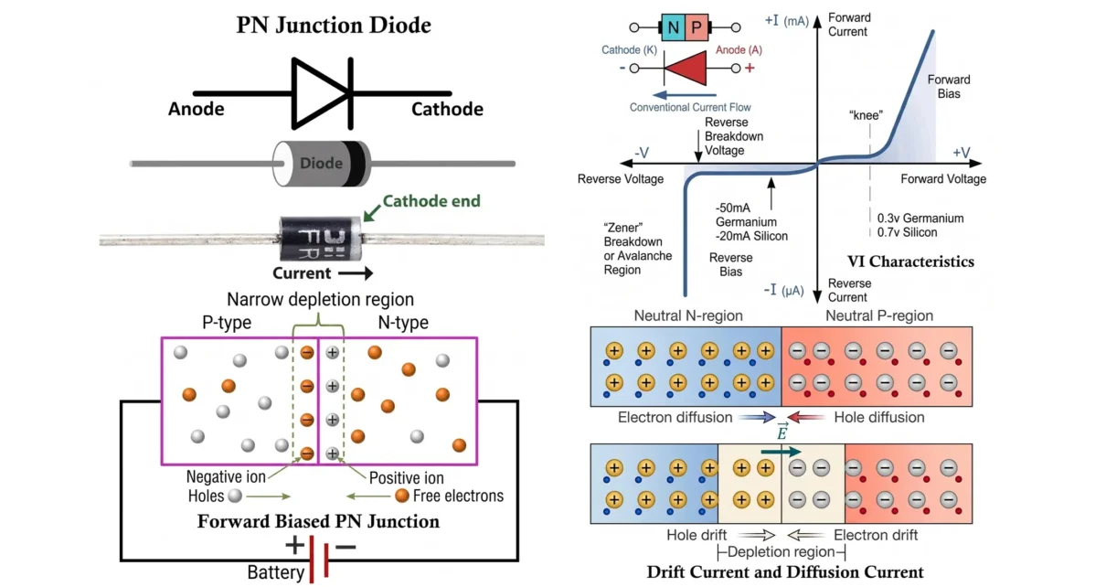
PN Junction Diode Symbol
The circuit symbol of a PN junction diode represents its two terminals and the direction of conventional current flow.

- The P-side is known as the Anode.
- The N-side is known as the Cathode.
- Conventional current flows from the anode to the cathode when the diode is forward biased.
In the symbol, the vertical line represents the cathode terminal, while the opposite side represents the anode terminal.
Construction of PN Junction Diode
A PN junction diode is manufactured from a single crystal of semiconductor material, typically silicon or germanium.
The fabrication process involves doping different portions of the semiconductor crystal with suitable impurities to create P-type and N-type regions.
P-Type Region: The P-type region is produced by adding trivalent impurities such as Boron, Gallium, Indium. These impurities create holes, which serve as the majority charge carriers in the P-region.
N-Type Region: The N-type region is formed by adding pentavalent impurities such as Phosphorus, Arsenic, Antimony. These impurities contribute free electrons, which become the majority charge carriers in the N-region.
Ohmic Contacts: Metal contacts are attached to both the P-region and N-region to connect the diode to an external circuit.
These contacts are known as Ohmic Contacts because:
- They allow current to flow equally in both directions.
- They introduce negligible voltage drop.
- They do not alter the electrical characteristics of the diode.
The contact connected to the P-region forms the anode, while the contact connected to the N-region forms the cathode.
Formation of PN Junction
When P-type and N-type semiconductor materials are joined together, charge carriers begin to move across the junction due to differences in their concentrations.

Diffusion of Electrons: The concentration of electrons is much higher in the N-region than in the P-region. As a result, electrons diffuse from the N-region to the P-region.
Diffusion of Holes: Similarly, the concentration of holes is much higher in the P-region than in the N-region. Therefore, holes diffuse from the P-region to the N-region.
This movement of charge carriers from a region of higher concentration to a region of lower concentration is known as diffusion.
Formation of Depletion Region
- As electrons leave the N-region and move into the P-region, positively charged donor ions are left behind.
- Likewise, when holes leave the P-region and move into the N-region, negatively charged acceptor ions remain behind.
- These fixed ions accumulate near the junction and create a region that is depleted of free charge carriers.
- This region is called the Depletion Region or Depletion Layer.

Characteristics of Depletion Region:
- It contains almost no free electrons or holes.
- It acts as an insulating barrier between the two regions.
- It opposes further diffusion of charge carriers.
- It plays a crucial role in determining the electrical behavior of the diode.
Barrier Potential
- The charged ions present in the depletion region generate an electric field across the junction.
- This electric field opposes the further movement of majority charge carriers across the junction.
- The voltage developed across the depletion layer due to this electric field is known as the Barrier Potential or Junction Potential.
- Silicon has a typical barrier potential of 0.7 V, while Germanium has a typical barrier potential of 0.3 V.

The barrier potential prevents majority carriers from crossing the junction under normal equilibrium conditions.
Working of PN Junction Diode
The operation of a PN junction diode can be understood through three different conditions.
A. Unbiased Condition
In the unbiased condition:
- No external voltage is applied.
- Diffusion current equals drift current.
- Net current is zero.
- A depletion region exists naturally at the junction.
B. Forward Bias Condition
In the forward-biased condition:
- P-side is connected to the positive terminal.
- N-side is connected to the negative terminal.
- Barrier potential decreases.
- Depletion region narrows.
- Majority carriers cross the junction.
- A large current flows through the diode.
Under these conditions, the diode behaves like a closed switch.
C. Reverse Bias Condition
In the reverse-biased condition:
- P-side is connected to the negative terminal.
- N-side is connected to the positive terminal.
- Barrier potential increases.
- Depletion region widens.
- Majority carriers cannot cross the junction.
- Only a tiny reverse saturation current flows.
Under these conditions, the diode behaves like an open switch.
Forward Bias vs Reverse Bias in Diode
The differences between forward bias and reverse bias are summarized in the table below:
| Parameter | Forward Bias | Reverse Bias |
|---|---|---|
| P-side Connection | Positive | Negative |
| N-side Connection | Negative | Positive |
| Barrier Potential | Decreases | Increases |
| Depletion Width | Decreases | Increases |
| Resistance | Low | Very High |
| Current Flow | Large | Very Small |
| Charge Carriers | Majority Carriers | Minority Carriers |
| Diode State | ON | OFF |
The unique ability of a PN junction diode to conduct current in one direction while blocking it in the opposite direction makes it one of the most important semiconductor devices in electronics. It is widely used in rectifiers, switching circuits, voltage protection systems, signal-processing applications, and many other electronic devices.
Unbiased PN Junction Diode
When no external voltage is applied across a PN junction diode, it is said to be in an unbiased condition.

Under this condition:
- Diffusion current exists because of majority carrier movement.
- Drift current exists because of minority carrier movement.
- Both currents are equal in magnitude.
- The net current through the diode is zero.
Diffusion Current: Diffusion current is produced by the movement of majority carriers from regions of higher concentration to regions of lower concentration.
Drift Current: Drift current is produced by the movement of minority carriers under the influence of the electric field present in the depletion region.

At equilibrium, the diffusion current and drift current balance each other. As a result, no external current flows through the diode.
Biasing of PN Junction Diode
The process of applying an external DC voltage across a PN junction diode is known as biasing. Biasing controls the flow of current through the diode and determines whether the diode will conduct or block current.
There are two types of biasing, forward biasing and reverse biasing. The behavior and operation of a PN junction diode depend entirely on these two biasing conditions.
Forward Biasing of PN Junction Diode
Forward biasing is the operating condition in which the P-region (anode) of a PN junction diode is connected to the positive terminal of a power supply, while the N-region (cathode) is connected to the negative terminal.
When connected in this manner, the externally applied voltage opposes the built-in barrier potential across the depletion region. As a result, the depletion layer becomes thinner, allowing charge carriers to cross the junction more easily and enabling current to flow through the diode.

Forward Bias Connection:
- P-region (Anode) → Positive terminal of the battery
- N-region (Cathode) → Negative terminal of the battery
This type of connection is known as forward biasing.
Forward Bias Circuit: In practical electronic circuits, a resistor is usually connected in series with the diode. This resistor limits the current flowing through the diode and protects it from excessive current that could cause damage.
Working of Forward-Biased PN Junction Diode
When a forward voltage is applied across the diode, the external electric field opposes the internal electric field created by the depletion region. As a result barrier potential decreases, width of the depletion region reduces and majority charge carriers move toward the junction. Initially, if the applied voltage is smaller than the barrier potential, very little current flows through the diode.
A) Applied Voltage Less Than Barrier Potential
When the forward voltage is less than the barrier potential, the applied voltage is not sufficient to overcome the junction barrier.
Under this condition:
- Electrons cannot move from the N-region to the P-region.
- Holes cannot move from the P-region to the N-region.
- Only a very small leakage current exists.
Therefore, the diode behaves almost like an open switch.
B) Applied Voltage Equal to Barrier Potential
As the forward voltage increases and approaches the barrier potential:
- The depletion region becomes extremely thin.
- The barrier potential is nearly neutralized.
- Majority carriers gain enough energy to cross the junction.
Typical barrier potential values are:
- Silicon diode: approximately 0.7 V
- Germanium diode: approximately 0.3 V
At this stage, noticeable conduction begins and the diode starts allowing significant current flow.
C) Applied Voltage Greater Than Barrier Potential
When the applied forward voltage becomes greater than the barrier potential, the depletion region becomes very narrow. As a result, a large number of majority charge carriers cross the junction, producing a substantial forward current.
Electron Flow: Free electrons move from N-region → P-region. After entering the P-region, these electrons recombine with holes and continue toward the positive terminal of the power supply.
Hole Flow: Holes move from P-region → N-region. The combined movement of electrons and holes produces a large forward current through the diode.
The forward current in a diode is mainly due to the movement of majority charge carriers. Electrons are the majority carriers in the N-region. Holes are the majority carriers in the P-region.
For this reason, forward conduction is often referred to as majority carrier conduction.
Effect of Forward Bias on the Depletion Region
One of the most important effects of forward biasing is the reduction in the width of the depletion layer. As electrons and holes move toward the junction, Positive ions in the N-region become neutralized. Negative ions in the P-region become neutralized. This process decreases the width of the depletion region.
- The depletion region becomes thinner.
- Junction resistance decreases.
- Current flow increases rapidly.
- The diode behaves like a closed switch.
Effect of Forward Bias on Barrier Potential
The externally applied forward voltage opposes the internal electric field of the junction. As a result, the barrier potential decreases.
When the barrier potential decreases:
- More charge carriers can cross the junction.
- Junction resistance becomes lower.
- Forward current increases rapidly.
The total forward voltage across the diode can be expressed as:
VF = VB + IF rf
- VF = Total forward voltage
- VB = Barrier potential
- IF = Forward current
- rf = Forward resistance
Silicon diode voltage drop ≈ 0.7 V, Germanium diode voltage drop ≈ 0.3 V.
Reverse Biasing of PN Junction Diode
Reverse biasing is the condition in which the P-region is connected to the negative terminal of the power supply and the N-region is connected to the positive terminal.
In this arrangement, the external voltage supports the barrier potential instead of opposing it. As a result depletion region becomes wider, junction resistance increases and current flow is almost completely blocked.

Reverse Bias Connection
- P-region (Anode) → Negative terminal
- N-region (Cathode) → Positive terminal
This arrangement is known as reverse biasing.
Working of Reverse-Biased PN Junction Diode
When reverse voltage is applied electrons in the N-region are attracted toward the positive terminal and holes in the P-region are attracted toward the negative terminal. Both types of majority charge carriers move away from the junction.
Since the charge carriers move away from the junction:
- Majority carrier conduction does not occur.
- The depletion layer expands.
- Junction resistance becomes extremely high.
As a result, the diode behaves almost like an open circuit.
Effect of Reverse Bias on the Depletion Region
The reverse voltage pulls charge carriers away from the junction. This action leaves behind additional uncovered ions on both sides of the junction. Consequently, the depletion region becomes wider, junction capacitance decreases and resistance increases significantly.
- Wider depletion layer
- Higher barrier potential
- Higher junction resistance
- Negligible current flow
Effect of Reverse Bias on Barrier Potential
Reverse bias increases the electric field across the junction. Therefore, the barrier potential increases. A higher barrier potential makes it extremely difficult for majority carriers to cross the junction. As a result, the diode remains in a non-conducting state under normal reverse-bias conditions.
Reverse Current in PN Junction Diode
Although majority carriers cannot cross the junction during reverse biasing, a very small current still flows through the diode. This current is produced by minority charge carriers.
Minority Carriers: Electrons in the P-region, Holes in the N-region
These minority carriers are generated due to thermal energy within the semiconductor material. The resulting current is known as the reverse saturation current, represented by IS.
Characteristics of Reverse Saturation Current:
- Very small in magnitude
- Nearly constant over a wide range of reverse voltages
- Independent of reverse voltage under normal conditions
- Strongly dependent on temperature
Typical reverse saturation current is in the nanoampere (nA) range for silicon diodes and in the microampere (μA) range for germanium diodes.
Because germanium diodes have a higher reverse saturation current than silicon diodes, they are generally more sensitive to temperature changes.
V-I Characteristics of PN Junction Diode
The relationship between the voltage applied across a PN junction diode and the current flowing through it is known as the Voltage-Current (V-I) Characteristics of the diode. These characteristics describe the electrical behavior of the diode under different biasing conditions and help determine important parameters such as cut-in voltage, forward resistance, reverse saturation current, and breakdown voltage.
The V-I characteristics of a PN junction diode are divided into two parts forward characteristics and reverse characteristics. These characteristics explain why a diode conducts current in one direction and blocks it in the opposite direction.
- Forward Region:
- Negligible current below cut-in voltage
- Rapid increase in current after the knee point
- Low forward resistance
- Reverse Region:
- Very small reverse saturation current
- Nearly constant current with increasing reverse voltage
- Sudden rise in current at breakdown voltage
These characteristics demonstrate the rectifying property of the diode, allowing current to flow easily in one direction while restricting it in the opposite direction.

Forward V-I Characteristics of PN Junction Diode
The forward V-I characteristic shows the relationship between the forward voltage (VF) applied across the diode and the forward current (IF) flowing through it.
In forward bias:
- The P-region is connected to the positive terminal of the supply.
- The N-region is connected to the negative terminal.
As the applied voltage increases, the depletion region narrows, allowing charge carriers to cross the junction more easily.
Region Before Cut-In Voltage
When the applied forward voltage is lower than the barrier potential, the depletion region still opposes the movement of charge carriers. As a result, only a negligible current flows through the diode.
Typical barrier potentials for silicon and germanium diodes are 0.7V and 0.3V. In this region, the diode is practically non-conducting.
Cut-In Voltage (Threshold Voltage)
The minimum forward voltage required to start significant conduction is called the Cut-In Voltage, Threshold Voltage, Knee Voltage, or Turn-On Voltage.
| Diode Material | Cut-In Voltage |
|---|---|
| Germanium (Ge) | 0.2–0.3 V |
| Silicon (Si) | 0.6–0.7 V |
At this voltage, the diode begins to conduct appreciable current.
Knee Point of the Characteristic Curve
The point at which the forward current starts increasing rapidly is known as the Knee Point.
Beyond the knee point:
- The depletion layer becomes very thin.
- Junction resistance decreases significantly.
- A small increase in voltage produces a large increase in current.
Most practical diode operations occur beyond this region.
Forward Conduction Region
Once the applied voltage exceeds the cut-in voltage, majority carriers cross the junction in large numbers and the diode conducts heavily.
Characteristics of this region include:
- Rapid increase in forward current
- Low junction resistance
- Exponential current growth with voltage
The forward current is described by the diode equation:
I = I₀ (e(V/ηVₜ) − 1)
- I = Diode current
- I₀ = Reverse saturation current
- V = Applied voltage
- η = Ideality factor
- Vₜ = Thermal voltage
This equation explains the exponential nature of the forward characteristic.
Forward Resistance of PN Junction Diode
The resistance offered by a diode during forward bias is called Forward Resistance. It is much smaller than the resistance offered during reverse bias.
Static Forward Resistance: Static forward resistance is the ratio of forward voltage to forward current at a particular operating point.
Rₓ = Vₓ / Iₓ
- Rₓ = Static forward resistance
- Vₓ = Forward voltage
- Iₓ = Forward current
Dynamic Forward Resistance: Dynamic resistance represents the small-signal resistance of the diode and is defined as the ratio of a small change in voltage to the corresponding change in current.
rₓ = ΔVₓ / ΔIₓ
It can also be expressed as the reciprocal of the slope of the forward characteristic curve. Dynamic resistance is generally very low in the normal operating region.
Reverse V-I Characteristics of PN Junction Diode
The reverse V-I characteristic shows the relationship between reverse voltage (VR) and reverse current (IR).
In reverse bias:
- The P-region is connected to the negative terminal.
- The N-region is connected to the positive terminal.
This increases the width of the depletion region and prevents the flow of majority carriers.
Reverse Saturation Current Region
Even under reverse bias, a very small current flows due to thermally generated minority carriers. This current is called the Reverse Saturation Current Iₛ.
Characteristics of reverse saturation current:
- Very small in magnitude
- Nearly independent of reverse voltage
- Strongly affected by temperature
- Caused by minority carriers
Typical values are:
| Diode Type | Reverse Saturation Current |
|---|---|
| Silicon | Few nA |
| Germanium | Few μA |
Because germanium diodes have higher leakage current, silicon diodes are preferred in most electronic applications.
Reverse Breakdown Region
As the reverse voltage increases, the reverse current remains nearly constant until a critical voltage is reached. Beyond this point, the diode enters the Breakdown Region. The voltage at which breakdown occurs is known as the Breakdown Voltage (VBR).
In the breakdown region:
- Reverse current increases sharply.
- Junction resistance decreases drastically.
- Excessive current may damage the diode if not limited.
Breakdown Mechanisms
Reverse breakdown can occur through two mechanisms.
A. Zener Breakdown
Zener breakdown occurs in heavily doped junctions with a very thin depletion layer.
- Strong electric field across the junction
- Electrons are pulled directly from covalent bonds
- Occurs at relatively low reverse voltages
- Common below 5–6 V
This effect is utilized in Zener diodes for voltage regulation.
B. Avalanche Breakdown
Avalanche breakdown occurs in lightly doped junctions at higher reverse voltages.
- Charge carriers gain high kinetic energy
- Collisions generate additional electron-hole pairs
- Multiplication of carriers causes a sudden rise in current
- This occurs at higher voltages and produces large reverse current
Comparison of Silicon and Germanium Diodes

| Parameter | Silicon Diode | Germanium Diode |
|---|---|---|
| Cut-In Voltage | 0.7 V | 0.3 V |
| Reverse Leakage Current | Very Low | Higher |
| Temperature Stability | Excellent | Poor |
| Breakdown Voltage | Higher | Lower |
| Power Handling | Better | Lower |
| Reliability | High | Moderate |
Silicon diodes are widely used because they offer lower leakage current, better temperature stability, higher reliability, and improved power-handling capability compared to germanium diodes.
Diode Current Equation (Shockley Equation)
The V-I characteristics of a PN junction diode can be described mathematically using the Diode Current Equation, also known as the Shockley Diode Equation.
This equation establishes the relationship between the voltage applied across the diode and the current flowing through it.
The diode current equation is given by:
I = Iₛ (e(V/ηVₜ) − 1)
- I = Current flowing through the diode (A)
- Iₛ = Reverse saturation current (A)
- V = Voltage across the diode (V)
- η = Ideality factor (Emission coefficient)
- Vₜ = Thermal voltage (V)
- e = Base of natural logarithm (≈ 2.718)
The Shockley equation accurately predicts the behavior of a diode in both forward-bias and reverse-bias conditions.
Ideality Factor (η)
The Ideality Factor, also called the Emission Coefficient, indicates how closely a practical diode follows the behavior of an ideal diode. It accounts for carrier recombination and other non-ideal effects occurring inside the semiconductor junction.
Typical Values of Ideality Factor:
| Diode Material | Ideality Factor (η) |
|---|---|
| Germanium Diode | 1 |
| Silicon Diode | 2 |
| Practical Diodes | 1 to 2 |
Importance of Ideality Factor:
- Determines the slope of the V-I curve.
- Influences forward current.
- Reflects recombination effects inside the depletion region.
- Indicates deviation from ideal diode behavior.
A smaller ideality factor results in faster current growth for a given forward voltage.
Thermal Voltage (Vₜ)
The thermal voltage represents the effect of temperature on the movement of charge carriers inside the semiconductor.
Vₜ = kT/q
- k = Boltzmann’s constant = 1.38 × 10⁻²³ J/K
- T = Absolute temperature (Kelvin)
- q = Electronic charge = 1.602 × 10⁻¹⁹ C
At room temperature (300 K): Vₜ ≈ 25.9 mV
Approximately: Vₜ ≈ 26 mV
Thermal voltage plays a crucial role in determining:
- Forward current
- Reverse saturation current
- Diode sensitivity to temperature
- Shape of the V-I characteristic curve
As temperature increases, thermal voltage also increases, affecting the overall behavior of the diode.
Significance of the Diode Current Equation
The diode equation explains several important characteristics of a PN junction diode:
- Forward current increases exponentially with voltage.
- Reverse current remains nearly constant.
- Diode current is strongly influenced by temperature.
- Silicon and germanium diodes exhibit different current responses.
- Small voltage changes can produce large current variations.
The equation forms the basis for analyzing and designing diode circuits.
Forward Bias Analysis Using Shockley Equation
In forward bias: V > 0, The exponential term becomes very large compared to 1.
Therefore: e(V/ηVₜ) >> 1
The equation simplifies to: I ≈ Iₛ e(V/ηVₜ)
This shows that the forward current increases exponentially with the applied voltage. This exponential relationship is responsible for the steep rise observed in the forward V-I characteristic curve after the knee voltage.
Reverse Bias Analysis Using Shockley Equation
In reverse bias: V < 0 The exponential term becomes extremely small.
Thus: e(V/ηVₜ) ≈ 0
The diode current equation becomes: I ≈ −Iₛ
This indicates that the reverse current remains approximately equal to the reverse saturation current. Hence, before breakdown, the reverse current remains almost constant regardless of the applied reverse voltage.
Effect of Temperature on V-I Characteristics
Temperature has a significant influence on the performance of a PN junction diode. As temperature rises, the number of thermally generated charge carriers increases, causing noticeable changes in diode characteristics.

Effect on Barrier Potential
The barrier potential decreases with increasing temperature.
Typical reduction: ≈ 2 mV/°C for Silicon Diodes
As a result, the diode turns ON at a lower voltage, forward conduction starts earlier and cut-in voltage decreases.
Effect on Reverse Saturation Current
Reverse saturation current increases rapidly with temperature. Reverse saturation current doubles for every 10°C rise in temperature.
Iₛ₂ = Iₛ₁ × 2(ΔT/10)
- Iₛ₁ = Initial reverse saturation current
- Iₛ₂ = Final reverse saturation current
- ΔT = Temperature change
This is one reason why semiconductor devices require proper thermal management.
Effect on Forward Characteristics
With increasing temperature:
- Forward current increases.
- Cut-in voltage decreases.
- Dynamic resistance decreases.
- Conduction becomes easier.
The forward V-I curve shifts toward the left.
Effect on Reverse Characteristics
As temperature increases:
- Reverse leakage current increases.
- Reverse saturation current becomes larger.
- Power dissipation increases.
- Risk of thermal runaway increases.
This effect is more pronounced in germanium diodes than in silicon diodes.
Diode Capacitance
Diode capacitance is the ability of a PN junction diode to store electric charge due to the presence of the depletion region and charge carriers.
Transition Capacitance (Junction Capacitance)
When a PN junction diode is reverse biased, the depletion region behaves like the dielectric of a capacitor. The P-region and N-region act as capacitor plates, while the depletion layer acts as the insulating medium.

This capacitance is known as:
- Transition Capacitance
- Junction Capacitance
- Depletion Capacitance
- Space-Charge Capacitance
- It is represented by CT
Transition Capacitance Formula
The transition capacitance is given by:
CT = εA/W
- ε = Permittivity of semiconductor material
- A = Junction area
- W = Width of depletion region
Effect of Reverse Voltage on Transition Capacitance
When reverse voltage increases, depletion width increases and capacitance decreases.
CT ∝ 1/W
This voltage-dependent capacitance is utilized in:
- Varactor diodes
- Electronic tuning circuits
- Voltage-controlled oscillators (VCOs)
- RF communication systems
Diffusion Capacitance
When a diode is forward biased, a large number of charge carriers are injected across the junction. These carriers are temporarily stored near the junction. The resulting charge-storage effect behaves like a capacitance known as diffusion capacitance or storage capacitance, it is represented by Cᴅ.

Diffusion Capacitance Formula
The diffusion capacitance is expressed as:
Cᴅ = τI/(ηVₜ)
- τ = Carrier lifetime
- I = Forward current
- η = Ideality factor
- Vₜ = Thermal voltage
Characteristics of Diffusion Capacitance
- Appears during forward bias.
- Increases with forward current.
- Much larger than transition capacitance.
- Important in high-frequency circuits.
- Affects switching speed of the diode.
Diffusion capacitance can range from nano-farads to microfarads depending on operating conditions.
Diode Models
To simplify circuit analysis, practical diodes are often replaced with equivalent circuit models. These models approximate the behavior of the diode under different operating conditions.
A. Ideal Diode Model
The ideal diode is considered a perfect switch.
- Forward Bias
- Acts as a short circuit.
- Zero voltage drop.
- Zero resistance.
- Reverse Bias
- Acts as an open circuit.
- Infinite resistance.
- No current flow.
Although no real diode behaves this way, the ideal model greatly simplifies basic circuit analysis.
B. Practical Diode Model
The practical model considers the cut-in voltage of the diode. The diode is represented as an ideal diode in series with a voltage source equal to the barrier potential. This model provides a more realistic approximation of actual diode behavior.
C. Complete Diode Model
The complete model includes:
- Cut-in voltage
- Forward resistance
- Reverse leakage current
The forward voltage is given by:
Vᶠ = Vᴮ + Iᶠrᶠ
- Vᴮ = Barrier potential
- Iᶠ = Forward current
- rᶠ = Forward resistance
This model closely matches the behavior of practical PN junction diodes and is commonly used in engineering calculations and circuit design.
Advantages of PN Junction Diode
- Simple Construction: Easy to manufacture and integrate into electronic circuits.
- Unidirectional Conduction: Allows current flow in one direction while blocking it in the opposite direction.
- High Reliability: Provides stable performance and long operational life.
- Low Cost: Economical semiconductor device widely available in the market.
- Fast Switching Capability: Suitable for high-speed electronic switching applications.
- Compact Size: Small physical dimensions make it suitable for modern electronic devices.
- Low Power Consumption: Requires relatively low power for operation.
- Wide Range of Applications: Used in rectification, signal processing, voltage regulation, protection circuits, and communication systems.
Disadvantages of PN Junction Diode
- Unidirectional Operation: Cannot conduct current in both directions like some other semiconductor devices.
- Forward Voltage Drop: Silicon diodes typically require about 0.7 V and germanium diodes about 0.3 V before significant conduction begins.
- Temperature Sensitivity: Electrical characteristics change with temperature.
- Limited Power Handling: Standard PN junction diodes may not handle very high currents or voltages.
- Reverse Breakdown Risk: Excessive reverse voltage can cause breakdown and damage if current is not limited.
- Nonlinear Characteristics: Circuit analysis becomes more complex due to exponential V-I behavior.
- Leakage Current: Small reverse saturation current flows even under reverse bias conditions.
Applications of PN Junction Diode
- Rectifiers: Conversion of AC to DC in power supplies.
- Switching Circuits: Used as electronic switches in digital and logic circuits.
- Voltage Regulation: Employed in voltage stabilization and protection circuits.
- Clipping Circuits: Used to limit signal amplitude to desired levels.
- Clamping Circuits: Used to shift the DC level of signals.
- Signal Detection and Demodulation: Widely used in communication systems.
- Protection Circuits: Protect sensitive components from reverse polarity and voltage spikes.
- Wave-Shaping Circuits: Used in pulse and waveform processing applications.
- Electronic Instruments: Found in measuring, testing, and control equipment.
- Computer and Electronics: Used extensively in modern electronic devices and integrated systems.
Conclusion
The PN junction diode is one of the most fundamental and important semiconductor devices in electronics. Its ability to conduct current in the forward direction and block it in the reverse direction makes it indispensable in electronic circuit design. Understanding its construction, working principles, V-I characteristics, biasing conditions, and practical behavior provides the foundation for studying advanced semiconductor devices such as transistors and integrated circuits. Due to its reliability, simplicity, and versatility, the PN junction diode continues to be widely used in power supplies, communication systems, signal-processing circuits, and countless electronic applications.
Here are some of the most popular PN junction diodes along with their datasheet PDF links.
- 1N4148 (Fast Switching Diode)
- 1N4007 (General Purpose Rectifier Diode)
- 1N4001–1N4007 Rectifier Series
- 1N4448 (High-Speed Switching Diode)
- 1N914 (Signal Switching Diode)
- 1N4148-1 (Military/Industrial Grade)
- LL4148 (SMD Version of 1N4148)
- 1N4007W (SMD Rectifier Diode)
Frequently Asked Questions (FAQs)
What is a PN junction diode?
A semiconductor device formed by joining P-type and N-type materials that allows current to flow mainly in one direction.
What is the function of the depletion region?
The depletion region acts as a barrier that controls charge-carrier movement and diode conduction.
What is the difference between forward bias and reverse bias?
Forward bias reduces the barrier potential and allows current flow. Reverse bias increases the barrier potential and blocks current flow.
What are the cut-in voltages of silicon and germanium diodes?
Approximately 0.7 V for silicon diodes and 0.3 V for germanium diodes.
What is reverse saturation current?
A small reverse-bias current caused by thermally generated minority carriers.
Why are silicon diodes more commonly used than germanium diodes?
They offer lower leakage current, better temperature stability, higher reliability, and greater power-handling capability.
What is breakdown voltage?
The reverse voltage at which heavy conduction begins due to Zener or avalanche breakdown.
What are the major applications of PN junction diodes?
Rectification, switching, voltage regulation, signal detection, clipping, clamping, and circuit protection.
What is the barrier potential of a PN junction diode?
The voltage across the depletion region that opposes majority-carrier movement; about 0.7 V for silicon and 0.3 V for germanium.
Why is a PN junction diode called a rectifier device?
Because it conducts in one direction and blocks in the other, enabling AC-to-DC conversion.
Types of Diodes: Symbol, Working, Characteristics and Applications
Light Emitting Diode LED – Symbol, Construction, Working, Types and Applications
Laser Diode – Symbol, Construction, Working, Types and Applications
Rectifier Circuit: Construction, Working, Types and Applications
Diode Clamper Circuit Diagram, Types, Working and Applications
Diode Clipper Circuit Diagram, Types, Working and Applications
