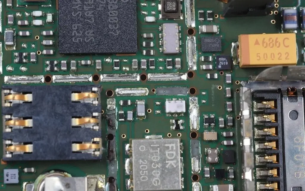
As modern electronics evolve toward becoming smaller, faster, and more powerful, the demand for compact and high-performance circuit boards has skyrocketed. It is where high-density interconnect (HDI) PCB manufacturing technology plays a pivotal role. HDI PCBs allow for more interconnections in a smaller footprint, making them ideal for smartphones, wearables, medical devices, and automotive electronics.
But what is a HDI PCB? A high-density interconnect PCB is a printed circuit board that integrates advanced features such as microvias, blind and buried vias, and via-in-pad technology to increase wiring density and enhance signal performance. These innovations allow designers to achieve more functionality in a reduced space without compromising speed or reliability.
Unlike traditional PCB manufacturing, the HDI PCB manufacturing process involves precise fabrication methods, including laser drilling, sequential lamination, and high-resolution imaging. Each step is engineered to support ultra-fine lines, tight tolerances, and complex layer structures which are critical elements for high-speed and high-frequency electronic applications.
In the following sections, we’ll explore the step-by-step manufacturing process of HDI PCBs, examine the technologies that make them possible, and break down the challenges and considerations that manufacturers face when building these advanced circuit boards.
Related Articles:
- PCB Manufacturing and Assembly Process
- Types of PCB Materials Their Properties and Applications
- How to Assemble Electronic Components on a PCB
- Cost-Effective Overseas PCB Services for Small Businesses
- Revolutionary Axial Flux Printed Circuit Board (PCB) Stator Motor
- High Speed PCB Design: Routing, Impedance & Layout Techniques
- What are the Key Stages in Aluminum PCB Manufacturing?
Overview of the HDI PCB Manufacturing Process
The term high-density interconnect (HDI) refers to a technology allowing higher wiring density per unit area on a printed circuit board (PCB). It is achieved through finer lines and spaces, smaller vias and capture pads, and higher connection pad density. HDI PCBs are essential in modern electronics where compact design and high performance go hand-in-hand. Smartphones, wearables, and automotive systems all benefit from HDI design.
So, what is a HDI PCB? Simply put, it’s a PCB that contains one or more of the following features:
- Microvias
- Blind and buried vias
- Via-in-pad structures
- Sequential lamination and stacking via configurations
Because HDI boards pack more functionality into smaller footprints, the PCB manufacturing process must be more precise, involving advanced fabrication techniques. Let’s walk through this process step-by-step.
HDI PCB Manufacturing Process
Each phase in HDI PCB manufacturing is crucial to ensuring electrical integrity, mechanical stability, and long-term reliability. Below is a breakdown of the key steps involved:
Design and CAD Modeling
Every successful HDI board starts with meticulous design. Using advanced CAD (Computer-Aided Design) software, engineers lay out the circuitry, determine the number of layers, and plan the via structures.
Key Design Considerations:
- Placement of microvias and via-in-pad configurations
- Impedance control for high-speed signals
- Layer stack-up for signal integrity and thermal performance
HDI design demands collaboration between design engineers and manufacturing teams to ensure feasibility and reduce prototyping time.
Lamination
Lamination is the process of bonding layers of conductive and insulating materials together to form the board’s structure. In high-density interconnect boards, lamination is more complex due to multiple layers and via structures.
Types of laminations in HDI:
- Sequential Lamination: Involves building the PCB in multiple cycles, typically used in multilayer HDI boards.
- Staggered and Stacked Vias: Requires precise alignment and controlled pressure and temperature.
The lamination stage determines the board’s mechanical strength and dimensional stability and must be conducted under stringent process controls.
Laser Drilling for Microvias
Microvias are tiny vias typically less than 150 microns in diameter, they are a defining feature of HDI boards. Laser drilling is employed because traditional mechanical drilling can’t achieve such precision.
Benefits of Laser Drilling in HDI:
- Enables high-density component placement
- Reduces signal path lengths, improving performance
- Supports miniaturization for compact applications
UV or CO₂ lasers are used depending on the material stack and via specifications. This non-contact drilling method ensures minimal mechanical stress and high accuracy.
Blind and Buried Vias Formation
Vias are the electrical connections between layers. In HDI PCB manufacturing, different types of vias are used to save space and improve signal integrity:
- Blind Vias: Connect outer layers to one or more inner layers, but do not go through the entire board.
- Buried Vias: Connect only to inner layers, which are not visible outside.
- Stacked Vias: Multiple microvias aligned vertically, enabling dense interconnects.
The correct via strategy allows for complex routing while maintaining the board’s compact size and performance.
Via Plating and Copper Deposition
After forming the vias, they must be plated with copper to establish solid electrical connections. It is done through electroplating or electroless copper deposition, which is especially important in HDI PCB due to its smaller diameters.
Copper Deposition Process:
- Cleaning and activating the via walls
- Applying a thin conductive seed layer
- Electroplating to build up the copper thickness
Plating must be uniform and void-free, especially in microvias, to ensure thermal and mechanical stress reliability.
Etching and Patterning
Once the copper layers are deposited, the circuit pattern is formed using photolithography and chemical etching. A photoresist layer is applied, exposed to UV light through a circuit mask, and developed to reveal the pattern.
Etching Considerations for HDI:
- Fine line/space resolution (often under 75 microns)
- Accurate control to prevent undercutting
- Clean and sharp trace edges to maintain signal quality
As HDI designs push for finer geometries, precision in this step is more critical than ever.
Soldermask Application
The soldermask is a protective coating applied over the circuit to insulate and prevent accidental solder bridging during component assembly. The mask must be aligned perfectly for HDI PCBs due to the high component density and fine features.
Types of Soldermask:
- Liquid Photo-imageable (LPI)
- Dry film solder mask (for very fine pitch designs)
Proper soldermask application prevents short circuits and helps maintain the long-term performance of the board.
Surface Finish
A surface finish is applied to exposed copper pads to protect them from oxidation and improve solderability.
Standard finishes used in HDI PCB manufacturing include:
- ENIG (Electroless Nickel Immersion Gold): Offers excellent flatness and long shelf life.
- OSP (Organic Solderability Preservative): Environmentally friendly and cost-effective.
- Immersion Silver or Tin: Used for high-reliability and fine-pitch requirements.
Surface finish choice affects everything from solder joint reliability to final product cost.
Final Inspection and Testing
Before shipping, HDI PCBs undergo rigorous quality checks to ensure that all circuits function correctly and meet customer specifications.
Inspection and testing methods:
- Automated Optical Inspection (AOI) for trace and component verification
- X-ray inspection for buried vias and solder joint analysis
- Electrical testing for continuity and shorts
These tests ensure that the board is defect-free and ready for the demanding applications for which HDI technology is known.
Technologies and Techniques Used in HDI PCB Manufacturing
Modern high-density interconnect (HDI) PCBs are only possible thanks to advanced technologies and innovative techniques. The precision required in HDI fabrication especially with microvias, fine lines, and thin substrates demands state-of-the-art equipment and specialized processes. Below are the key technologies that enable high-performance HDI PCB manufacturing.
Laser Drilling
Laser drilling is one of the most critical processes in HDI production. It creates microvias that are significantly smaller than standard vias and enables high-density component placement.
Benefits of laser drilling:
- Extreme precision (typically 20–150 µm in diameter)
- Minimal thermal and mechanical stress
- Compatibility with sequential build-up (SBU) technology
Lasers are also ideal for drilling blind and buried vias, especially in multilayer printed circuit boards with complex stack-ups.
Through-Hole vs. Microvia
Traditional through-hole vias span the entire PCB thickness and are suitable for basic interlayer connections. However, HDI PCBs use microvias due to their smaller size, lower parasitic inductance, and better electrical performance.
Microvias are:
- Shorter, reducing signal loss
- Easier to place under fine-pitch components
- Ideal for multilayer PCB manufacturing where space is at a premium
Understanding the distinction is crucial when planning an HDI board’s design and layer stack.
Stacked Vias
In complex HDI boards, microvias are often stacked vertically to form high-density interconnections. This process, known as via stacking, allows for:
- Increased routing density
- Vertical interconnects across multiple layers
- Compact form factors for portable electronics
Proper alignment and plating of stacked vias are essential for maintaining electrical continuity and mechanical reliability.
HDI PCB Lamination Process
The lamination process in HDI manufacturing is more intricate than that of standard PCBs due to sequential build-up (SBU) layers. Each layer is built and laminated separately, then drilled and plated before the next layer is added.
Key aspects of HDI lamination:
- High-pressure, high-temperature cycles
- Alignment systems to prevent registration errors
- Careful control of resin flow to avoid defects
Proper lamination ensures mechanical integrity and signal consistency across layers.
Via Filling
Filling microvias with conductive or non-conductive material is another unique requirement in HDI PCB manufacturing. It is crucial when using via-in-pad designs or stacked microvias.
Why via filling is essential:
- Prevents solder wicking during assembly
- Increases mechanical strength of the via
- Creates a planar surface for BGA and fine-pitch components
Conductive via filling is often used when stacked vias require continuous electrical pathways.
Challenges in HDI PCB Manufacturing
Despite their advantages, HDI PCBs present several manufacturing challenges that must be managed carefully to ensure a successful end product. Below are some of the most common issues engineers and manufacturers face when producing HDI boards.
Manufacturing Complexity
HDI fabrication involves:
- Multiple lamination cycles
- Microvia drilling and plating
- Fine-pitch patterning
- Complex layer alignment
Each of these steps requires precision and control, increasing the difficulty and length of the PCB manufacturing process. Advanced automation and skilled technicians are essential to maintaining high yields and consistent quality.
Cost
While HDI PCBs deliver superior performance, they are generally more expensive to produce due to:
- Specialized materials (e.g., high-Tg laminates)
- Advanced processes like laser drilling and sequential lamination
- Higher inspection and testing requirements
Cost optimization strategies include careful layer stack planning, panel optimization, and early design-for-manufacturing (DFM) collaboration.
Material Selection
Choosing the right materials for high-density interconnect boards is critical. Materials must:
- Support high thermal stability (for lead-free assembly)
- Offer low dielectric loss (for high-speed signals)
- Have matched coefficients of thermal expansion (CTE)
Improper material selection can lead to warping, delamination, or reduced signal integrity.
Via Integrity
Due to their small size, microvias are more susceptible to issues like voiding, cracks and incomplete plating. Ensuring integrity requires precise drilling, effective cleaning, high-quality copper plating, and regular inspection via X-ray or cross-section analysis.
Quality Control and Testing
HDI boards must pass stringent quality checks before deployment. This is due to their use in critical, high-performance applications.
Testing methods include:
- Automated Optical Inspection (AOI) for pattern verification
- X-ray Inspection for hidden via and solder joint assessment
- Electrical Testing for open/short detection
In addition, flex and stress testing may be used, particularly for boards in dynamic environments like wearables or aerospace systems.
HDI PCB Types
High-density interconnect (HDI) PCBs are classified into three types based on the structure and the number of layers in which microvias and vias are used. Understanding these types is crucial for choosing the correct type of HDI PCB for specific applications.
Type 1 HDI
Type 1 HDI PCBs are the simplest form of HDI boards and typically consist of a single layer of microvias on one or both sides of the board. These boards are commonly used for low- to medium-density interconnect applications, where simplicity and cost-effectiveness are essential.
Characteristics of Type 1 HDI:
- Typically used in single- or double-sided applications
- Features blind microvias (vias that connect only one layer)
- Minimal use of sequential lamination
These boards are ideal for applications such as simple consumer electronics or low-density circuits where fewer connections are needed.
Type 2 HDI
Type 2 HDI PCBs represent a more advanced level of complexity. These boards feature microvias and buried vias, allowing interconnections between inner layers. Type 2 HDI PCBs typically require at least two lamination cycles, allowing for more layers and complex routing.
Features of Type 2 HDI:
- Microvias and buried vias
- Greater layer count and routing density
- Typically used in more advanced electronics like smartphones and industrial controls
This is the most common type used in medium to high-density applications, balancing complexity, performance, and cost.
Type 3 HDI
Type 3 HDI PCBs are the most advanced and complex, featuring stacked microvias and via-in-pad technologies. It allows for the highest-density interconnections and is typically used in high-performance applications like mobile devices, high-frequency circuit boards, and advanced networking equipment.
Characteristics of Type 3 HDI:
- Microvias, buried vias, and stacked vias
- High-density routing, often with multiple sequential lamination cycles
- Requires advanced manufacturing technologies like laser drilling and precise lamination
These PCBs are designed for the most demanding applications that require high-speed signal transmission and minimal footprint.
Common Surface Finishes for HDI PCBs
Once the HDI PCB is completed, a surface finish is applied to the exposed copper pads to enhance solderability, prevent oxidation, and ensure high-quality solder joints. Depending on the application’s requirements, several surface finishes are commonly used in HDI PCB manufacturing.
ENIG (Electroless Nickel Immersion Gold)
ENIG is one of HDI PCBs’ most widely used surface finishes, especially for high-performance and high-reliability applications. It involves depositing a thin layer of gold over a nickel layer.
Benefits of ENIG:
- Excellent corrosion resistance and solderability
- Flat and smooth surface for fine-pitch components
- Long shelf life
ENIG is often used for advanced electronics like smartphones, automotive systems, and medical devices where reliable solder joints are critical.
HASL (Hot Air Solder Leveling)
HASL is a traditional surface finish that involves dipping the PCB into molten solder and then using hot air to level the solder over the exposed copper. It is often used in high-volume manufacturing due to its simplicity and cost-effectiveness.
Advantages of HASL:
- Reliable and cost-effective
- Suitable for most general-purpose HDI PCBs
- Provides good solderability
However, HASL can have some limitations with very fine-pitch components due to the roughness of the finish, which is why it’s typically used for less complex HDI applications.
OSP (Organic Solderability Preservative)
OSP is an environmentally friendly surface finish option that involves applying a thin layer of organic material to the copper to protect it from oxidation. This finish is often chosen for lower-cost applications where fine-pitch components are not required.
Benefits of OSP:
- Environmentally friendly and cost-effective
- It provides excellent solderability when properly managed
- Suitable for lower-density HDI boards
While OSP is less robust than ENIG or HASL in high-reliability applications, it’s perfect for consumer electronics with less demanding performance needs.
Final Quality Control
Once the HDI PCB has undergone the necessary fabrication steps, it must pass a series of final quality control (QC) checks to ensure it meets the required performance standards. Their use in high-performance, mission-critical applications like telecommunications and medical devices is particularly critical for HDI PCBs.
Automated Optical Inspection (AOI)
Automated Optical Inspection (AOI) uses high-resolution cameras and software to inspect the HDI PCB for defects. It compares the board against pre-defined design rules to check for:
- Misalignment of layers
- Solder bridge detection
- Trace continuity and short circuits
AOI is essential for ensuring that each board meets the stringent requirements for high-density interconnections.
X-ray Inspection
X-ray inspection is beneficial for inspecting hidden vias and solder joints in HDI PCBs, particularly for stacked vias or via-in-pad designs that can’t be checked visually. This technique allows for the internal structure of the PCB to be analyzed without damaging the board.
Benefits of X-ray inspection:
- Detects hidden defects like voids in vias and under-filled vias
- Essential for multilayer boards and high-density interconnects
- Improves the quality and reliability of HDI PCB manufacturing
X-ray ensures that critical areas of the board, especially in multilayer configurations, are free from defects.
Electrical Testing
Electrical testing involves verifying that all electrical pathways on the HDI PCB are correct and that there are no open circuits or shorts. This test is critical for confirming that the board functions as intended before it leaves the factory.
Common methods include:
- In-circuit testing (ICT) Measures each connection on the board
- Functional testing: Tests the board in a real-world application
- Flying probe testing: Uses probes to test individual points on the board for continuity and shorts
Electrical testing ensures that the HDI PCB will perform reliably under operational conditions, assuring the manufacturer and the end user.
Revolutionary Axial Flux Printed Circuit Board (PCB) Stator Motor
High Speed PCB Design: Essential Wiring Techniques for Optimal Performance
