This article covers the 555 Timer IC in detail, including its pin configuration, internal block diagram, working principle, operating modes, formulas, waveform analysis, advantages, disadvantages, and applications.
The 555 Timer IC is one of the most widely used integrated circuits in electronics. Developed in 1971 by Hans Camenzind at Signetics, it is designed for generating precise time delays, oscillations, pulses, and switching signals.
Due to its simple design, low cost, stability, and versatility, the 555 Timer IC is used in a wide range of applications such as LED flashers, alarm systems, PWM circuits, oscillators, motor controllers, embedded systems, robotics, automotive electronics, and consumer devices.
The IC operates in three main modes Monostable mode, Astable mode, Bistable mode. Its internal structure combines comparators, a flip-flop, transistors, resistors, and output circuitry within a single package, allowing it to perform multiple timing and waveform-generation functions efficiently.
The name “555” comes from the three internal 5 kΩ resistors used in its voltage divider network. Even decades after its introduction, the IC remains one of the most popular timing circuits in the electronics industry because of its reliability and ease of implementation.
555 Timer IC Pin Diagram
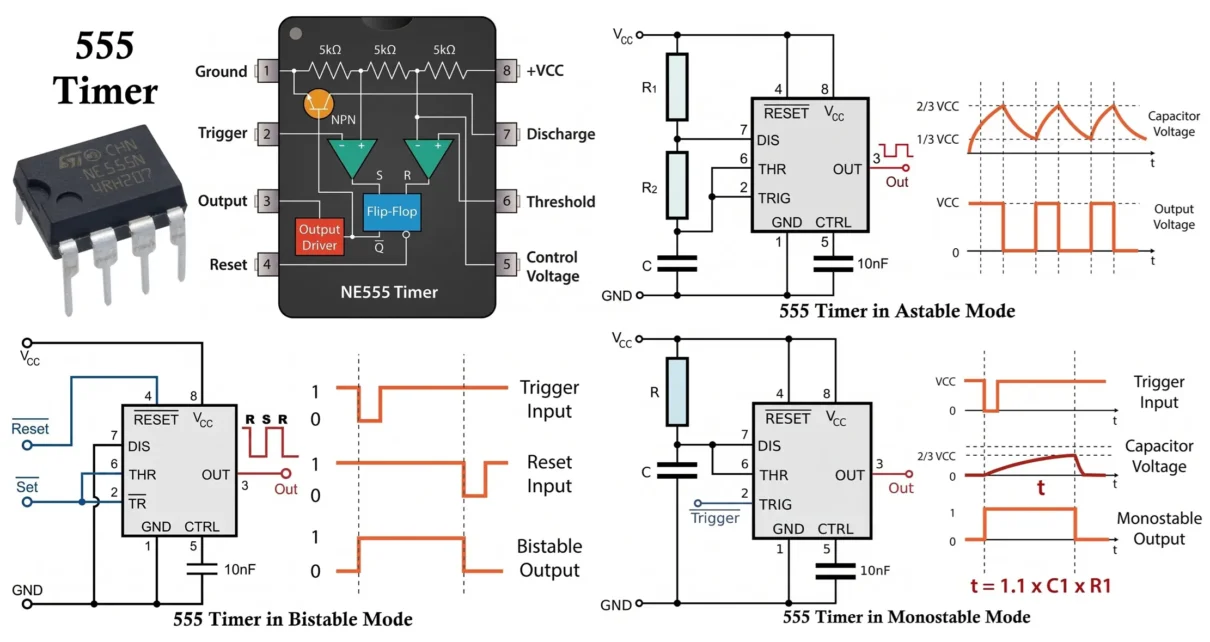
The 555 Timer IC is available in an 8-pin package. Each pin performs a specific function in the operation of the IC.

| Pin Number | Pin Name | Function |
|---|---|---|
| 1 | Ground (GND) | Connected to ground |
| 2 | Trigger | Starts timing cycle |
| 3 | Output | Output signal terminal |
| 4 | Reset | Resets the IC |
| 5 | Control Voltage | Controls threshold level |
| 6 | Threshold | Ends timing cycle |
| 7 | Discharge | Discharges capacitor |
| 8 | VCC | Positive supply voltage |
Related Articles:
- DC-DC Boost Converter Circuit Using 555 Timer
- PIR Motion Sensor Circuit with 555 Timer IC
- LED Chaser Circuit using 555 Timer and CD4017 IC
- Brushless DC – BLDC Motor Driver Circuit using 555 Timer IC
- 12V to 230V Inverter Circuit Diagram using 555 timer IC
- 4 Easy Clap Switch Circuits with 555 Timer, 4017 IC & Transistors
- Voltage Controlled Oscillator VCO Circuit Using 555 Timer IC
555 Timer IC Pin Description

Pin 1 Ground (GND)
This pin is connected to the negative terminal of the power supply. It acts as the reference point for the entire circuit.
- Connected directly to ground
- Provides common return path
- Usually connected to 0V
Pin 2 Trigger Pin
The trigger pin activates the timer operation. The timer gets triggered when the voltage at this pin falls below 1/3Vcc.
- Active LOW input
- Connected to comparator
- Starts timing cycle
VTrigger < 1/3 VCC
When this condition occurs, the output becomes HIGH.
Pin 3 Output Pin
This is the output terminal of the IC.
- Can source or sink current
- Output current capability is approximately 200mA
- Used to drive LEDs, relays, speakers, motors, and logic circuits
The output alternates between HIGH and LOW states depending on the operating mode.
Pin 4 Reset Pin
The reset pin is used to reset the timer manually.
- Active LOW pin
- When connected to ground, the output becomes LOW
- Usually connected to VCC when not used
Condition for reset:
VRESET < 0.7V
Pin 5 Control Voltage Pin
This pin provides access to the internal voltage divider network.
- Modifies threshold voltage
- Used in modulation applications
- Helps generate PWM signals
Normally, a small capacitor of 0.01µF is connected to ground to reduce noise.
Pin 6 Threshold Pin
The threshold pin monitors capacitor voltage. When the voltage exceeds the threshold, output becomes LOW and the discharge transistor turns ON.
VTHRESHOLD > 2/3 VCC
Pin 7 Discharge Pin
The discharge pin provides a path for capacitor discharge through an internal transistor.
- Discharges timing capacitor
- Controls oscillation cycle
- Important in astable and monostable operation
Pin 8 VCC Pin
This pin supplies power to the IC.
Typical supply voltage range:
4.5V ≤ VCC ≤ 18V
Internal Block Diagram of 555 Timer IC
The 555 Timer IC is a highly popular timing device used for generating delays, pulses, and oscillations. Internally, the 555 Timer IC contains:
- 25 Transistors
- 15 Resistors
- 2 Diodes
- 2 Comparators
- SR Flip-Flop
- Output Driver Stage
- Discharge Transistor

These internal sections work together to control the charging and discharging of an external capacitor. The internal block diagram of the 555 timer mainly consists of the following functional sections:
- Voltage Divider Network
- Lower Comparator
- Upper Comparator
- SR Flip-Flop
- Discharge Transistor
- Output Driver Stage

Voltage Divider Network
Inside the IC, three 5 kΩ resistors are connected in series between VCC and ground. This resistor network divides the supply voltage into two fixed reference voltages 1/3Vcc and 2/3Vcc. These reference voltages are supplied to the two internal comparators. The name “555 timer” actually comes from these three 5 kΩ resistors.
Lower Comparator (Trigger Comparator)
The lower comparator compares the voltage at the Trigger pin (Pin 2) with the 1/3Vcc reference voltage. When the trigger voltage becomes lower than 1/3Vcc, the comparator output becomes HIGH. This sets the SR flip-flop.
- The output pin becomes HIGH
- The discharge transistor turns OFF
- The external capacitor starts charging
Thus, the lower comparator is responsible for starting the timing cycle.
Upper Comparator (Threshold Comparator)
The upper comparator compares the voltage at the Threshold pin (Pin 6) with the 2/3Vcc reference voltage. When the threshold voltage exceeds 2/3Vcc, the comparator resets the SR flip-flop.
- The output pin to become LOW
- The discharge transistor to turn ON
- The external capacitor to discharge
Therefore, the upper comparator terminates the timing interval.
SR Flip-Flop
The SR flip-flop acts as the memory section of the IC. It stores the current state of the timer.
- The lower comparator SETS the flip-flop
- The upper comparator RESETS the flip-flop
Depending on the state of the flip-flop, the output stage and discharge transistor change their operation. The flip-flop ensures stable switching between HIGH and LOW output states.
Discharge Transistor
The discharge transistor is internally connected to Pin 7. Its function is to discharge the external timing capacitor whenever the output becomes LOW.
When the transistor turns ON, the capacitor gets connected to ground and discharges rapidly. When the transistor turns OFF, the capacitor is allowed to charge through external resistors.
This charging and discharging process forms the basis of timing operations in the 555 timer.
Output Driver Stage
The output driver stage is built using multiple transistors connected in a push-pull arrangement. This stage provides high current driving capability.
Unlike ordinary logic ICs, the 555 timer can directly drive components such as LEDs, Relays, Buzzers, small Speakers. The output stage can both source and sink current, making the IC suitable for many practical applications.
Working of the 555 Timer IC
The working of the 555 Timer IC is based on the charging and discharging cycle of an external capacitor. Internally, the IC uses comparators, an SR flip-flop, and a discharge transistor to control this operation.

Capacitor Voltage Below 1/3 VCC: When the capacitor voltage falls below 1/3 VCC, the lower comparator becomes active and sets the SR flip-flop. As a result, the output becomes HIGH and the discharge transistor turns OFF. Since the discharge transistor is OFF, the external capacitor starts charging through the external resistor.
Capacitor Charging: As the capacitor charges, its voltage gradually increases from 1/3 VCC toward 2/3 VCC. During this interval, the output remains HIGH and the discharge transistor stays OFF.
Capacitor Voltage Reaches 2/3 VCC: When the capacitor voltage becomes greater than 2/3 VCC, the upper comparator becomes active and resets the SR flip-flop. This makes the output LOW and turns ON the discharge transistor.
Capacitor Discharging: Once the discharge transistor turns ON, the capacitor gets connected to ground through Pin 7 and starts discharging. As the capacitor voltage decreases below 1/3 VCC, the lower comparator again sets the flip-flop and the cycle repeats continuously.
This continuous charging and discharging process enables the NE555 Timer IC to generate time delays, pulses, square waves, and oscillations.
Operating Modes of 555 Timer IC
The 555 Timer IC can operate in three different modes depending on the external circuit connections:
- Astable Mode
- Monostable Mode
- Bistable Mode
Each mode performs a different function and is widely used in timing and pulse-generation applications.
Astable Mode (Free-Running Mode)
In astable mode, the 555 timer continuously switches between HIGH and LOW states without requiring any external triggering signal. Since there is no stable state, this mode is called astable.
In this mode, the capacitor continuously charges and discharges between 1/3 VCC and 2/3 VCC. Initially, the capacitor charges through resistors RA and RB. When the capacitor voltage reaches 2/3 VCC, the output becomes LOW and the discharge transistor turns ON. The capacitor then discharges through resistor RB.

When the capacitor voltage falls below 1/3 VCC, the output again becomes HIGH and the charging cycle repeats continuously. This process generates a square-wave output.
The pulse width or output time period is given by:
T = 1.1RC
The charging time is:
TH = 0.693(RA + RB)C
The discharging time is:
TL = 0.693RBC
The total time period is:
T = 0.693(RA + 2RB)C
The frequency of oscillation is:
f = 1.44 / (RA + 2RB)C
Duty cycle:
D = [(R1 + R2) / (R1 + 2R2)] × 100%
Applications of Astable Mode:
- Clock pulse generation
- LED flashers
- Tone generators
- PWM circuits
- Frequency generators
- Astable multivibrator circuit
- Square-wave oscillators
Monostable Mode (One-Shot Mode)
In monostable mode, the 555 timer produces a single output pulse for a fixed time duration whenever it receives a trigger signal. This mode has only one stable state, which is why it is called monostable.

Initially, the output remains LOW. When a negative trigger pulse is applied to the Trigger pin and the voltage falls below 1/3 VCC, the internal flip-flop gets set. The output becomes HIGH and the timing capacitor starts charging through the resistor.
As the capacitor voltage reaches 2/3 VCC, the upper comparator resets the flip-flop. The output then returns LOW and the capacitor discharges through the discharge transistor.
The pulse width or output time period is given by:
T = 1.1RC
- T = Output pulse duration
- R = External resistance
- C = External capacitance
The output pulse duration depends on the values of the resistor and capacitor connected externally.
Applications of Monostable Mode:
- Time delay circuits
- Pulse generation
- Touch switches
- Missing pulse detectors
- Debouncing circuits
- Automatic switching systems
Bistable Mode (Flip-Flop Mode)
In bistable mode, the 555 timer has two stable states: HIGH and LOW. In this mode, no capacitor is required for timing operation. The output changes state only when external trigger or reset signals are applied.

- A trigger pulse sets the output HIGH
- A reset pulse makes the output LOW
Since the output remains permanently in either state until another input signal is applied, the circuit behaves like a memory element or flip-flop. Unlike monostable and astable modes, bistable mode does not generate timing pulses automatically.
Applications of Bistable Mode:
- Toggle switches
- Memory storage circuits
- Push-button ON/OFF circuits
- Alarm control systems
- Digital switching applications
Due to these three versatile operating modes, the NE555 Timer IC is widely used in electronic timing, pulse generation, waveform generation, and control applications.
Advantages of NE555 Timer IC
- Simple Circuit Design: The 555 timer requires only a few external components such as resistors and capacitors, making circuit design simple, compact, and easy to implement.
- Low Cost and Easy Availability: The IC is inexpensive and readily available in the market, which makes it suitable for educational, industrial, and commercial applications.
- Highly Versatile Operation: The 555 timer can operate as a timer, oscillator, pulse generator, flip-flop, and PWM controller, allowing it to perform multiple functions within a single circuit.
- High Output Current Capability: The IC can source and sink relatively high current, enabling it to directly drive LEDs, relays, buzzers, and small loads without additional driver circuits.
- Reliable and Stable Performance: The timer provides stable timing operation and dependable performance even during continuous operation.
- Easy Interfacing: The IC can easily interface with analog and digital circuits such as logic gates, sensors, counters, and microcontrollers.
Disadvantages of NE555 Timer IC
- Limited Timing Accuracy: The timing accuracy depends mainly on external resistor and capacitor values, so component tolerances can affect the output timing.
- Not Suitable for Precision Applications: The 555 timer is less accurate compared to crystal oscillators and microcontroller-based timing systems.
- Higher Power Consumption: Standard bipolar versions of the IC consume more power compared to CMOS timer circuits.
- Output Noise: The output waveform may contain switching noise and voltage fluctuations in sensitive electronic circuits.
- Limited High-Frequency Operation: The IC is not ideal for very high-frequency applications because of internal switching limitations.
Applications of NE555 Timer IC
- Timing and Delay Circuits: The 555 timer is widely used for generating accurate time delays in relay delay circuits, sequential timers, and automatic control systems.
- Pulse and Waveform Generation: In astable mode, the IC generates continuous square waves and pulse signals used in clock circuits and frequency generators.
- LED Flashers and Blinking Circuits: The timer is commonly used in LED flashing and decorative lighting circuits due to its continuous ON/OFF pulse generation capability.
- PWM and Motor Speed Control: The IC generates PWM signals that are used to control DC motor speed and LED brightness.
- Alarm and Security Systems: The timer is used in burglar alarms, warning systems, emergency indicators, and siren circuits.
- Audio and Tone Generation: The 555 timer can generate audio-frequency signals used in buzzers, tone generators, and siren circuits.
- Robotics and Embedded Systems: The IC is widely used in robotics and embedded electronics for timing control, pulse generation, and signal conditioning applications.
Important Practical Notes
Use of Decoupling Capacitor: A small capacitor, typically 0.01 µF, is connected between Pin 5 (Control Voltage pin) and ground to suppress noise and improve stable operation of the timer.
Proper Reset Pin Connection: If the Reset pin (Pin 4) is not used in the circuit, it should always be connected directly to VCC to prevent unwanted resetting due to electrical noise.
Improving Timing Accuracy: The accuracy of the timer mainly depends on the external RC network. Using precision resistors and low-tolerance capacitors helps achieve more accurate and stable timing performance.
Power Consumption in CMOS Versions: CMOS variants such as the TLC555 consume significantly lower power compared to the standard bipolar NE555 timer, making them suitable for battery-operated and low-power applications.
Avoiding Noise Near Supply Pins: For better performance, a bypass capacitor is often connected between VCC and ground close to the IC to reduce supply voltage fluctuations and switching noise.
Heat and Frequency Considerations: At very high frequencies or heavy output loads, the IC may generate heat and timing stability may reduce. Proper operating limits should therefore be maintained for reliable performance.
Popular Variants of 555 Timer IC
| IC Number | Description |
|---|---|
| NE555 | Standard bipolar version |
| SE555 | Military-grade version |
| LM555 | Commercial timer IC |
| TLC555 | CMOS low-power version |
| ICM7555 | Precision CMOS timer |
Monostable vs Astable vs Bistable Modes of 555 Timer
| Parameter | Monostable | Astable | Bistable |
|---|---|---|---|
| Stable States | One | None | Two |
| External Trigger | Required | Not Required | Required |
| Oscillation | No | Yes | No |
| Capacitor Required | Yes | Yes | Usually No |
| Main Use | Time Delay | Oscillator | Flip-Flop |
Conclusion
The NE555 Timer IC is one of the most widely used and versatile integrated circuits in electronics. Its internal structure combines analog comparators, an SR flip-flop, resistor networks, and transistor switching circuits within a single compact package, allowing it to perform a variety of timing and waveform-generation functions efficiently.
The IC operates by controlling the charging and discharging cycle of an external capacitor, which enables it to generate accurate delays, pulses, square waves, and oscillations. With its ability to operate in monostable, astable, and bistable modes, the 555 timer can be adapted for numerous analog and digital applications.
It’s simple circuit design, low cost, reliable operation, and minimal external component requirement make it highly suitable for students, hobbyists, industrial designers, and professional engineers. From LED flashers and alarm systems to PWM controllers and oscillator circuits, the 555 timer continues to remain a fundamental building block in modern electronic circuit design.
Voltage Controlled Oscillator VCO Circuit Using 555 Timer IC
