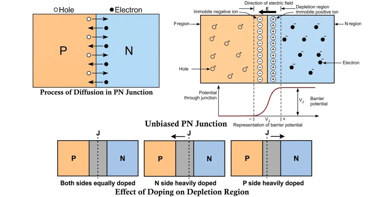
A PN junction is one of the most important structures in semiconductor electronics. It forms the basic building block of many electronic devices such as diodes, transistors, LEDs, solar cells, rectifiers, and integrated circuits. When a P-type semiconductor and an N-type semiconductor are joined together without applying any external voltage, the junction is called an […]
Tag: Depletion Width Formula
MOS Capacitor and MOS Capacitance CV Curves Explained
The MOS Capacitor (Metal Oxide Semiconductor Capacitor) is the fundamental electrostatic structure underlying modern semiconductor devices. Every MOSFET, CMOS integrated circuit, DRAM cell, Flash memory array, and nanoscale logic transistor originates from MOS capacitor physics. Understanding MOS capacitor behavior, electrostatics, energy band behavior, and Capacitance Voltage (CV) characteristics is essential for: Semiconductor device physics VLSI […]

