Embedded systems are becoming increasingly sophisticated. From smart home devices and industrial controllers to wearable medical equipment and automotive electronics, modern embedded products are expected to deliver more functionality within smaller form factors than ever before.
At the same time, advances in processors, wireless connectivity, artificial intelligence, and edge computing are pushing hardware designers to integrate more components onto limited board space. Traditional PCB technologies often struggle to meet these requirements without increasing board size, layer count, or manufacturing complexity.
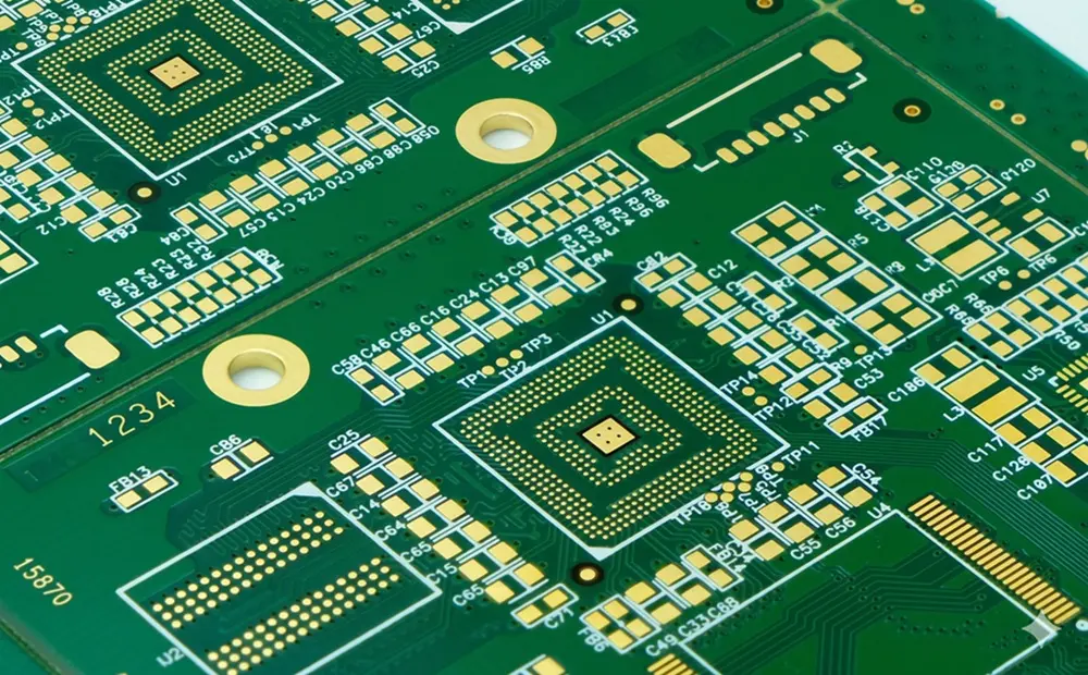
This is where High-Density Interconnect (HDI) PCB technology plays a crucial role. By enabling higher routing density, improved signal performance, and compact layouts, HDI PCBs have become a foundational technology for next-generation embedded systems.
Related Articles:
- PCB Manufacturing and Assembly Process
- RF Microwave PCB Design and Manufacturing Guide
- High-Density Interconnect (HDI) PCB Manufacturing Process
- Types of PCB Materials Their Properties and Applications
- How to Assemble Electronic Components on a PCB
- Cost-Effective Overseas PCB Services for Small Businesses
- Revolutionary Axial Flux Printed Circuit Board (PCB) Stator Motor
- High Speed PCB Design: Routing, Impedance & Layout Techniques
- What are the Key Stages in Aluminum PCB Manufacturing?
What Is HDI PCB Technology?
HDI, or High-Density Interconnect, refers to a PCB manufacturing approach that allows significantly higher wiring density compared to conventional printed circuit boards. HDI boards achieve this through advanced fabrication techniques such as:
- Microvias
- Blind vias
- Buried vias
- Fine-pitch traces
- Sequential lamination processes
These features enable designers to route more signals in less space while maintaining electrical performance and reliability. Compared with traditional PCBs, HDI boards can accommodate complex circuits without requiring larger board dimensions. This makes them particularly valuable for embedded systems where space is often limited.
Why Embedded Systems Need HDI PCBs
The demand for HDI technology is closely linked to the rapid evolution of embedded electronics. Today’s embedded products typically integrate:
- Multi-core processors
- Wireless communication modules
- Sensors
- Memory components
- Power management circuits
All of these components compete for space on the PCB.
According to the International Data Corporation (IDC), the global number of connected IoT devices is expected to exceed 40 billion within the next few years, driving demand for increasingly compact and intelligent embedded hardware. As more devices become connected, designers must fit greater functionality into smaller products without compromising performance. HDI PCB technology addresses this challenge by maximizing routing efficiency and component density.
For many advanced applications, working with an experienced HDI PCB manufacturer early in the design process helps engineers optimize stack-up structures, microvia placement, and routing strategies before production begins. This collaboration can significantly improve manufacturability while reducing redesign cycles.
Benefits of HDI PCBs for Embedded Systems
Reduced Product Size
One of the biggest advantages of HDI technology is miniaturization. Microvias occupy significantly less space than traditional through-hole vias, allowing more routing channels between components. Designers can therefore place components closer together and reduce overall board dimensions.
This benefit is especially important for:
- Wearable devices
- Medical sensors
- Consumer electronics
- Portable industrial equipment
As product sizes continue to shrink, HDI architecture becomes increasingly necessary.
Improved Signal Integrity
Modern embedded systems frequently support high-speed interfaces such as:
- DDR memory
- PCIe
- USB4
- Gigabit Ethernet
- MIPI interfaces
At higher frequencies, signal quality becomes a major concern.
HDI boards help maintain signal integrity by:
- Shortening signal paths
- Reducing parasitic capacitance
- Minimizing impedance discontinuities
- Lowering electromagnetic interference (EMI)
The result is more reliable communication between components and improved system performance.
Better Power Distribution
As embedded processors become more powerful, power integrity becomes increasingly important. HDI technology allows engineers to dedicate routing layers more efficiently, improving power delivery networks and reducing voltage fluctuations across the board.
Stable power distribution directly contributes to:
- Higher system reliability
- Improved processor performance
- Reduced electromagnetic noise
- Longer product lifespan
Increased Reliability
Modern HDI manufacturing processes are highly mature and capable of supporting demanding industrial applications.
Properly designed HDI boards can offer:
- Improved thermal management
- Enhanced mechanical durability
- Reduced routing congestion
- Better manufacturing consistency
These characteristics make HDI technology suitable for mission-critical embedded systems operating in challenging environments.
How HDI PCBs Support Modern Embedded Processors
The rise of powerful microcontrollers and System-on-Chip (SoC) devices has dramatically increased routing complexity.
Many modern processors feature:
- Hundreds of I/O pins
- Fine-pitch BGA packages
- Multiple memory interfaces
- High-speed communication channels
Routing these devices using traditional PCB techniques often results in larger boards and higher layer counts.
Fine-Pitch BGA Routing
Ball Grid Array (BGA) packages are commonly used in embedded computing platforms because they provide high pin density within compact footprints.
However, escaping signals from tightly packed BGA arrays can be extremely challenging.
HDI microvias enable designers to route signals directly from inner rows of BGA packages, dramatically increasing routing efficiency.
This capability allows:
- Smaller PCB footprints
- Lower layer counts
- Improved signal quality
- Reduced manufacturing costs
Supporting Edge AI Hardware
Edge AI applications are becoming a major driver of embedded system innovation.
Market research from Gartner indicates that a growing percentage of enterprise-generated data is now processed at the edge rather than in centralized cloud environments. This trend is increasing demand for compact AI-capable devices.
Edge AI processors often require:
- High-speed memory connections
- Multiple sensor interfaces
- Wireless connectivity modules
HDI PCB technology provides the routing density needed to integrate these features into compact products.
Applications of HDI PCB Technology
Internet of Things (IoT)
IoT devices require compact form factors while supporting wireless communication, sensors, and local processing.
Examples include:
- Smart home hubs
- Asset tracking devices
- Environmental monitoring sensors
- Smart meters
HDI technology enables these products to remain small while delivering advanced functionality.
Industrial Automation
Industrial embedded systems continue to become more intelligent and connected.
Common applications include:
- Programmable Logic Controllers (PLCs)
- Robotics controllers
- Machine monitoring systems
- Industrial gateways
HDI PCBs support the higher processing power and communication requirements of modern Industry 4.0 solutions.
Medical Electronics
Medical equipment places particularly high demands on size, reliability, and performance.
Examples include:
- Portable diagnostic devices
- Patient monitoring systems
- Wearable health trackers
- Imaging equipment control modules
HDI architecture helps manufacturers achieve compact designs without sacrificing reliability.
Automotive Electronics
The automotive industry is increasingly dependent on embedded computing systems.
Advanced Driver Assistance Systems (ADAS), telematics platforms, infotainment systems, and electric vehicle controllers all require high-density electronic assemblies.
HDI PCBs help automotive manufacturers meet strict performance and space constraints while maintaining reliability under demanding operating conditions.
Manufacturing Considerations for HDI PCB Projects
While HDI technology offers significant advantages, successful implementation requires careful planning.
Design for Manufacturability (DFM)
Engineers should consider manufacturing requirements from the earliest design stages.
Important factors include:
- Via structures
- Layer stack-ups
- Trace widths
- Material selection
- Assembly requirements
DFM reviews can identify potential manufacturing issues before production begins.
Material Selection
Different embedded applications require different material properties.
Designers should evaluate:
- Signal performance
- Thermal conductivity
- Mechanical stability
- Environmental resistance
Selecting appropriate materials helps maximize long-term reliability.
Partnering With the Right Manufacturer
HDI fabrication involves advanced manufacturing processes that require specialized expertise and equipment.
Choosing a manufacturing partner with proven HDI experience can help ensure:
- Accurate microvia formation
- Consistent impedance control
- Reliable layer registration
- High production yields
This becomes increasingly important as embedded systems continue to grow in complexity.
Future Trends in HDI PCB and Embedded Systems
Several technology trends are expected to accelerate HDI adoption in the coming years.
- Edge AI Expansion: As AI workloads move closer to end users, embedded hardware will require even greater routing density and processing capability.
- 5G and Advanced Wireless Connectivity: Next-generation wireless technologies demand improved RF performance and more sophisticated PCB layouts.
- Advanced Packaging Technologies: System-in-Package (SiP), chiplet architectures, and heterogeneous integration are driving higher interconnect density requirements.
- Continued Miniaturization: Consumers and industries alike continue to demand smaller products with greater functionality. HDI technology is uniquely positioned to support this long-term trend.
Conclusion
As embedded systems become more powerful, connected, and compact, PCB technology must evolve alongside them. HDI PCBs provide the routing density, signal integrity, and design flexibility required to support modern processors, wireless communication modules, and advanced embedded applications. From IoT devices and industrial automation equipment to medical electronics and automotive systems, HDI technology has become a key enabler of next-generation hardware innovation. Organizations that embrace HDI design principles today will be better prepared to meet the increasing performance and miniaturization demands of tomorrow’s embedded systems.
High Speed PCB Design: Essential Wiring Techniques for Optimal Performance
Revolutionary Axial Flux Printed Circuit Board (PCB) Stator Motor
